SLVSAG3A September 2010 – December 2014 TPS61252
PRODUCTION DATA.
- 1 Features
- 2 Applications
- 3 Description
- 4 Typical Application Schematic
- 5 Revision History
- 6 Device Options
- 7 Pin Configuration and Functions
- 8 Specifications
- 9 Parameter Measurement Information
- 10Detailed Description
- 11Application and Implementation
- 12Power Supply Recommendations
- 13Layout
- 14Device and Documentation Support
- 15Mechanical, Packaging, and Orderable Information
Package Options
Mechanical Data (Package|Pins)
- DSG|8
Thermal pad, mechanical data (Package|Pins)
- DSG|8
Orderable Information
8 Specifications
8.1 Absolute Maximum Ratings
over operating free-air temperature range (unless otherwise noted)(1)| MIN | MAX | UNIT | ||
|---|---|---|---|---|
| Voltage(2) | VIN, VOUT, SW, EN, PG, FB, ILIM | –0.3 | 7 | V |
| Temperature | Operating junction, TJ | –40 | 150 | °C |
| Storage, Tstg | –65 | 150 | ||
(1) Stresses beyond those listed under absolute maximum ratings may cause permanent damage to the device. These are stress ratings only, and functional operation of the device at these or any other conditions beyond those indicated under recommended operating conditions is not implied. Exposure to absolute-maximum-rated conditions for extended periods my affect device reliability.
(2) All voltages are with respect to network ground terminal.
8.2 ESD Ratings
| VALUE | UNIT | |||
|---|---|---|---|---|
| V(ESD) | Electrostatic discharge | Human-body model (HBM), per ANSI/ESDA/JEDEC JS-001(1) | ±2000 | V |
| Charged-device model (CDM), per JEDEC specification JESD22-C101(2) | ±500 | |||
(1) JEDEC document JEP155 states that 500-V HBM allows safe manufacturing with a standard ESD control process. Manufacturing with less than 500-V HBM is possible with the necessary precautions.
(2) JEDEC document JEP157 states that 250-V CDM allows safe manufacturing with a standard ESD control process. Manufacturing with less than 250-V CDM is possible with the necessary precautions.
8.3 Recommended Operating Conditions
| MIN | NOM | MAX | UNIT | |
|---|---|---|---|---|
| Supply voltage at VIN | 2.3 | 6.0 | V | |
| Output voltage at VOUT | 3.0 | 6.5 | V | |
| Programmable valley switch current limit set by RILIM | 100 | 1500 | mA | |
| Operating free air temperature range, TA | –40 | 85 | °C | |
| Operating junction temperature range, TJ | –40 | 125 | °C |
8.4 Thermal Information
| THERMAL METRIC(1) | TPS61252 | UNIT | |
|---|---|---|---|
| DSG | |||
| 8 PINS | |||
| RθJA | Junction-to-ambient thermal resistance | 80.2 | °C/W |
| RθJC(top) | Junction-to-case (top) thermal resistance | 93.5 | |
| RθJB | Junction-to-board thermal resistance | 54.2 | |
| ψJT | Junction-to-top characterization parameter | 0.9 | |
| ψJB | Junction-to-board characterization parameter | 59.3 | |
| RθJC(bot) | Junction-to-case (bottom) thermal resistance | 20 | |
(1) For more information about traditional and new thermal metrics, see the IC Package Thermal Metrics application report, SPRA953.
8.5 Electrical Characteristics
Over recommended free air temperature range, typical values are at TA = 25°C. Unless otherwise noted, specifications apply for condition VIN = EN = 3.6 V, VOUT = 5.0 V.8.6 Typical Characteristics
Table 1. Table of Graphs
| DESCRIPTION | FIGURE | |
|---|---|---|
| Efficiency | vs Output current (VOUT = 5.0 V, ILIM = 1.5 A) | Figure 1 |
| vs Output current in 100% Duty-Cycle Mode (VOUT = 5.0 V, ILIM = 1.5 A) | Figure 2 | |
| vs Input voltage (VOUT = 5.0 V, ILoad = {10; 100; 1000 mA}) , ILIM = 1.5 A | Figure 3 | |
| Maximum output current | vs Input voltage (VOUT = 5.0 V) | Figure 4 |
| Output voltage | vs Output current (VOUT = 5.0V, ILIM = 1.5 A) | Figure 5 |
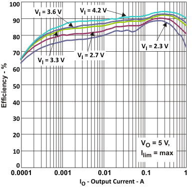 Figure 1. Efficiency vs Output Current
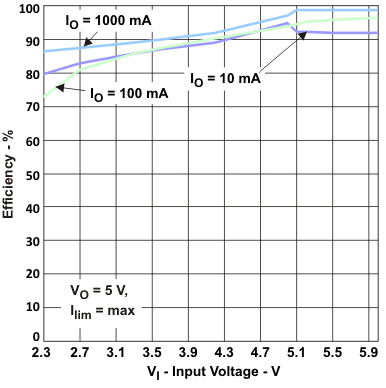 Figure 3. Efficiency vs Input Voltage
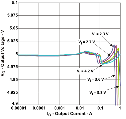 Figure 5. Output Voltage vs Output Current
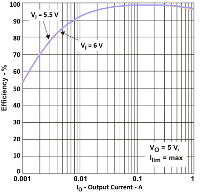 Figure 2. Efficiency vs Output Current
In 100% Duty Cycle Mode
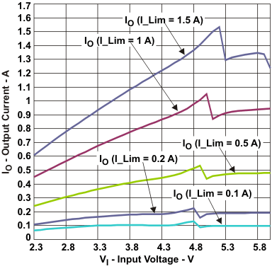 Figure 4. Maximum Output Current vs Input Voltage