SLVSBX9A September 2014 – September 2014 TPS61291
PRODUCTION DATA.
- 1 Features
- 2 Applications
- 3 Description
- 4 Revision History
- 5 Pin Configuration and Functions
- 6 Specifications
- 7 Detailed Description
- 8 Applications and Implementation
- 9 Power Supply Recommendations
- 10Layout
- 11Device and Documentation Support
- 12Mechanical, Packaging, and Orderable Information
Package Options
Mechanical Data (Package|Pins)
- DRV|6
Thermal pad, mechanical data (Package|Pins)
- DRV|6
Orderable Information
5 Pin Configuration and Functions
DRV Package
6 Pin
Top View
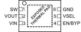
Pin Functions
| PIN | I/O | DESCRIPTION | |
|---|---|---|---|
| NAME | NO. | ||
| SW | 1 | I | Switch node of the converter. Connect the inductor between this pin and the input capacitor CIN. |
| VOUT | 2 | O | Boost converter output. Connect the output capacitor COUT between this pin and GND close to the device. |
| VIN | 3 | PWR | Input voltage supply pin for the boost converter. Connect the input capacitor CIN between this pin and GND as close as possible to the device. |
| EN/BYP | 4 | I | Control pin of the device. A high level enables the boost mode operation. A low level disables the boost converter and enables bypass mode operation. EN/BYP must be actively terminated high or low. Usually, this pin is controlled by the MCU in the system. |
| VSEL | 5 | I | Output voltage selection pin. The logic level of this pin is read out during startup and internally latched. Connect this pin only to GND, VOUT, or leave it floating. |
| GND | 6 | PWR | Ground pin of the device. |
| EXPOSED THERMAL PAD | NC | Not electrically connected to the IC, but must be soldered to achieve specified thermal performance. Connect this pad to the GND pin and use it as a central GND plane. | |