SLVSEL7B April 2019 – October 2019 TPS61390
PRODUCTION DATA.
- 1 Features
- 2 Applications
- 3 Description
- 4 Revision History
- 5 Pin Configuration and Functions
- 6 Specifications
- 7 Detailed Description
-
8 Application and Implementation
- 8.1 Application Information
- 8.2
Typical Application
- 8.2.1 Design Requirement
- 8.2.2
Detailed Design Procedure
- 8.2.2.1 Selecting the Rectifier Diode
- 8.2.2.2 Selecting the Inductor
- 8.2.2.3 Selecting Output Capacitor
- 8.2.2.4 Selecting Filter Resistor and Capacitor
- 8.2.2.5 Setting the Output Voltage
- 8.2.2.6 Selecting Sample Window
- 8.2.2.7 Selecting Capacitor for CAP pin
- 8.2.2.8 Selecting Capacitor for AVCC pin
- 8.2.2.9 Selecting Capacitor for APD pin
- 8.2.2.10 Selecting the Resistors of MON1 or MON2
- 8.2.2.11 Selecting the Capacitors of MON1 or MON2
- 8.2.2.12 Selecting the Resistor of Gain pin
- 8.2.2.13 Selecting the Short Current Limit
- 8.2.3 Application Curves
- 9 Power Supply Recommendations
- 10Layout
- 11Device and Documentation Support
- 12Mechanical, Packaging, and Orderable Information
Package Options
Mechanical Data (Package|Pins)
- RTE|16
Thermal pad, mechanical data (Package|Pins)
- RTE|16
Orderable Information
7.3.4 Sample and Hold
The TPS61390 has the sample-and-hold circuitry built in, including a holdup capacitor for storing the voltage capture, a FET switch, and one operational amplifier, illustrated in Functional Block Diagram.
To sample the current mirror signal, the switch connects the capacitor to the input of the common-mode operational amplifier. The amplifier converts the voltage of the capacitor to the output terminal with 4:1 ratio.
In hold mode the switch disconnects the hold-up capacitor from the operation amplifier, the voltage of the capacitor is discharged to 0 before connecting with current mirror output terminal (MON1 and MON2).
These are two ratios of the current mirror that can be selected automatically by comparing the MON1 voltage with the internal 400-mV reference. The voltage of MON1 is sampled if the MON1 voltage is below 400 mV, while the voltage of MON2 is sampled if MON1 being larger than 400 mV. The GAIN pin reports which ratio is selected for the sample and hold, the logic low (0) for MON1 while logic high (AVCC) for MON2 selected.
Also, the GAIN can be externally selected, pulling low to select the 1 : 5 while high for 4 : 5 ratio.
The voltage measured on VSP pin is calculated by Equation 1 and Equation 2 :

where
- VSP is the voltage sampled on VSP pin
- IAPD is the current flowing through the APD pin.
- RMON1 is the resistor connecting with MON1 pin
- IBIAS is the bias current of current mirror

where
- RMON2 is the resistor connecting with MON2 pin
The bias current is around 20 µA (typical) when there is no APD current flowing through. The bias voltage of MON1 or MON2 is 60 mV given a 3-kΩ MON resistor connected with MON1 or MON2. Also, the VSP voltage is reset to 250 mV prior to every sample clock coming. The maximum voltage of the MON1 is clamped to 400 mV while maximum of MON2 is 2.5 V. The maximum voltage of VSP is close to the AVCC (0.1 V lower typically), which is the supply voltage of the sample and hold circuitry.
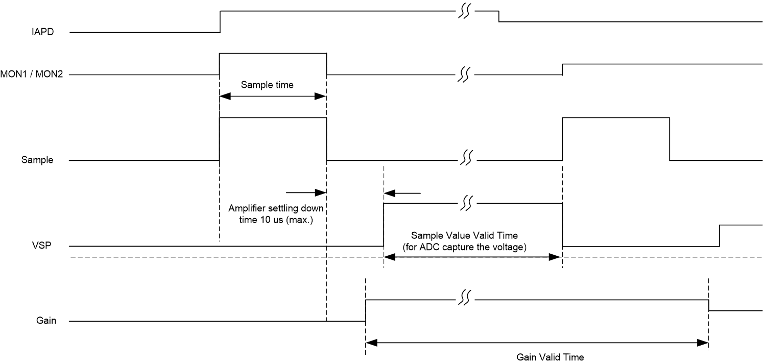
As the timing diagram shown in Figure 11, the sample and hold is enabled by the rising edge of an external clock connecting to the SAMPLE pin, the holdup capacitor captures the voltage of current mirror signal (the voltage of MON1 and MON2).
At the falling edge, the sampling is stopped, and the voltage stored on the holdup capacitor is transferred to the output of the operational amplifier. The minimum time of the sampling time the TPS61390 supports is 350 ns (typically). The voltage on the stored capacitor is switched to the amplifier’s input voltage. There is approximately 10-µs delay time to make the output voltage of the amplifier ready.
The GAIN selector is always active and the GAIN value is captured by the falling edge of the sample signal.
 Figure 11. TPS61390 Sample / Hold Circuit Timing
 The output settling time of the operational amplifier is 10 µs while the maximum duration time is 100 µs with 1% derating (with the nominal voltage).