SLVSFE7 November   2019 TPS61391

PRODUCTION DATA.  

  1. Features
  2. Applications
  3. Description
    1.     Device Images
      1.      Typical Application Circuit
  4. Revision History
  5. Pin Configuration and Functions
    1.     Pin Functions
  6. Specifications
    1. 6.1 Recommended Operating Conditions
    2. 6.2 Absolute Maximum Ratings
    3. 6.3 ESD Ratings
    4. 6.4 Thermal Information
    5. 6.5 Electrical Characteristics
    6. 6.6 Typical Characteristics
  7. Detailed Description
    1. 7.1 Overview
    2. 7.2 Functional Block Diagram
    3. 7.3 Feature Description
      1. 7.3.1 Undervoltage Lockout
      2. 7.3.2 Enable and Disable
      3. 7.3.3 Current Mirror
      4. 7.3.4 High Optical Power Protection
    4. 7.4 Device Functional Mode
      1. 7.4.1 PFM Operation
  8. Application and Implementation
    1. 8.1 Application Information
    2. 8.2 Typical Application
      1. 8.2.1 Design Requirement
      2. 8.2.2 Detailed Design Procedure
        1. 8.2.2.1  Selecting the Rectifier Diode
        2. 8.2.2.2  Selecting the Inductor
        3. 8.2.2.3  Selecting Output Capacitor
        4. 8.2.2.4  Selecting Filter Resistor and Capacitor
        5. 8.2.2.5  Setting the Output Voltage
        6. 8.2.2.6  Selecting Capacitor for CAP pin
        7. 8.2.2.7  Selecting Capacitor for AVCC pin
        8. 8.2.2.8  Selecting Capacitor for APD pin
        9. 8.2.2.9  Selecting the Resistors of MON1 or MON2
        10. 8.2.2.10 Selecting the Capacitors of MON1 or MON2
        11. 8.2.2.11 Selecting the Short Current Limit
      3. 8.2.3 Application Curves
  9. Power Supply Recommendations
  10. 10Layout
    1. 10.1 Layout Guidelines
    2. 10.2 Layout Example
  11. 11Device and Documentation Support
    1. 11.1 Documentation Support
      1. 11.1.1 Related Documentation
    2. 11.2 Receiving Notification of Documentation Updates
    3. 11.3 Support Resources
    4. 11.4 Trademarks
    5. 11.5 Electrostatic Discharge Caution
    6. 11.6 Glossary
  12. 12Mechanical, Packaging, and Orderable Information
    1. 12.1 Package Option Addendum
      1. 12.1.1 Packaging Information
      2. 12.1.2 Tape and Reel Information

Package Options

Mechanical Data (Package|Pins)
Thermal pad, mechanical data (Package|Pins)
Orderable Information

Typical Characteristics

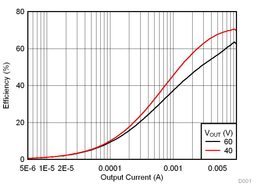
TPS61391 D001_SLVSEL7.gif
VIN = 3.3 V L = 4. 7 µH COUT = 0.1 µF
Output current (boost) = 0 to 8 mA
Figure 1. Efficiency vs. Output Current
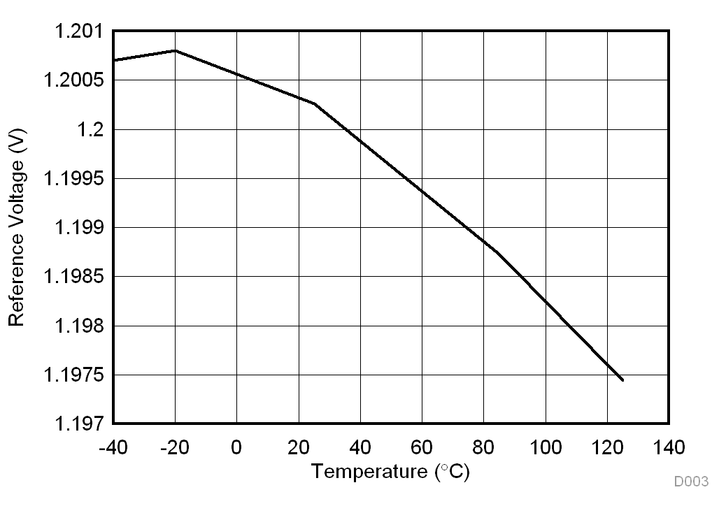
TPS61391 D003_SLVSEL7.gif
VIN = 3.3 V VOUT = 60 V COUT = 0.1 µF
Figure 3. Reference voltage
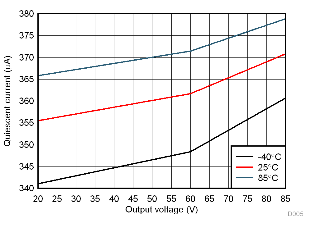
TPS61391 D005_SLVSEL7.gif
VIN = 3.3 V
Figure 5. Quiescent current vs. Output voltage
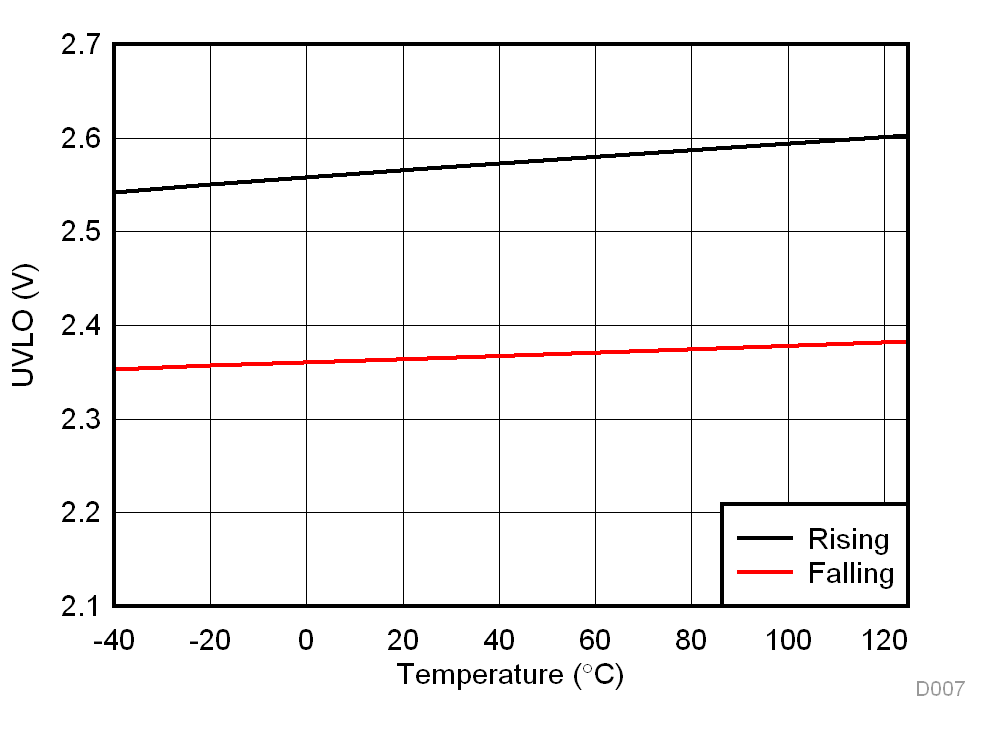
TPS61391 D007_SLVSEL7.gif
VOUT = 60 V
Figure 7. Vin UVLO
TPS61391 D009_SLVSEL7.gif
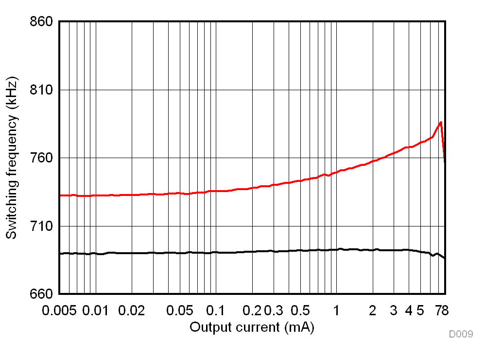
VIN = 3.3 V VOUT = 60 V
Figure 9. Switching frequency vs. Output current
TPS61391 D002_SLVSEL7.gif
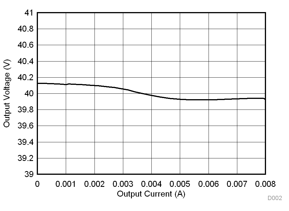
VIN = 3.3 V L = 4. 7 µH COUT = 0.1 µF
Output current (boost) = 0 to 8 mA
Figure 2. Load regulation
TPS61391 D004_SLVSEL7.gif
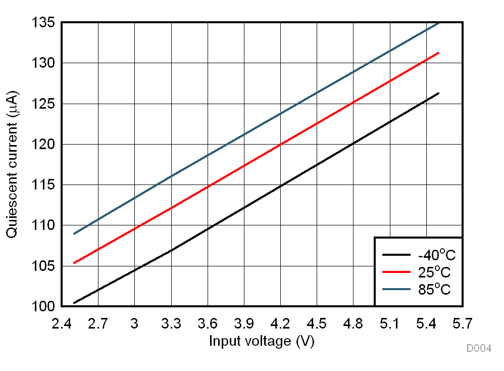
VOUT = 60 V
Figure 4. Quiescent current vs. Input voltage
TPS61391 D006_SLVSEL7.gif
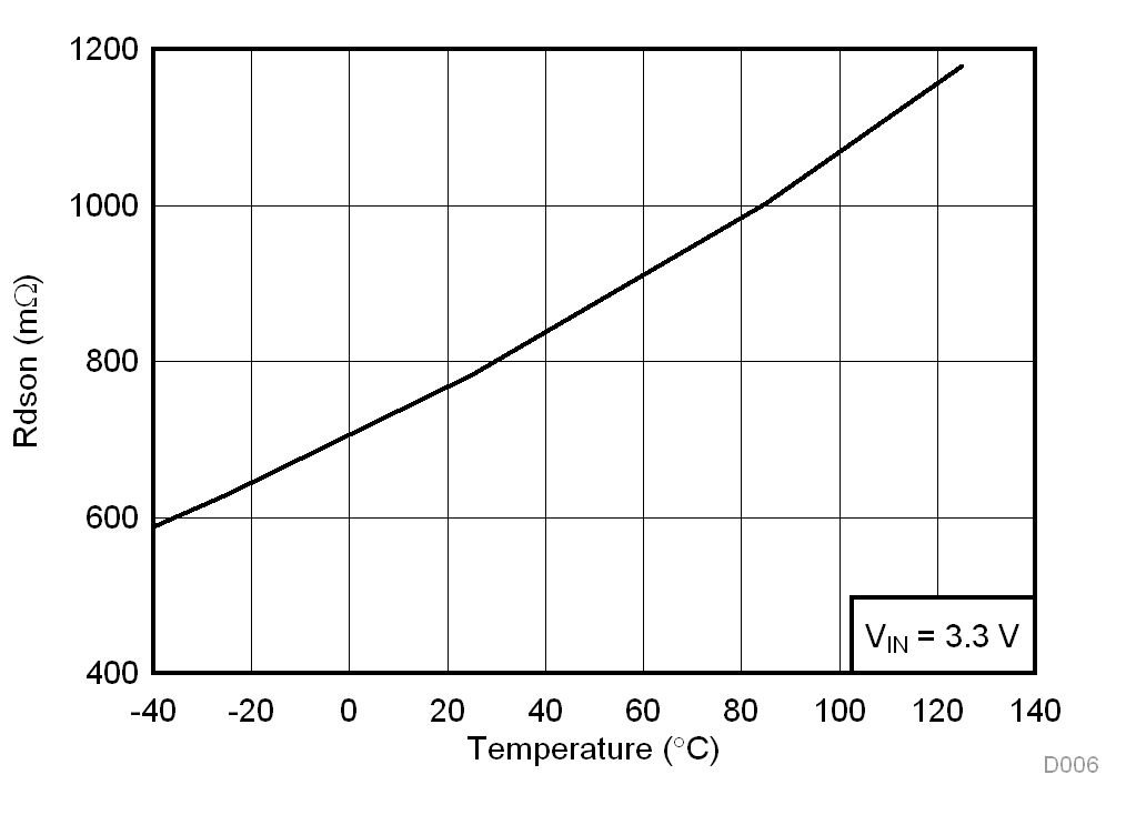
VIN = 3.3 V VOUT = 60 V
Figure 6. Rdson vs. Temperature
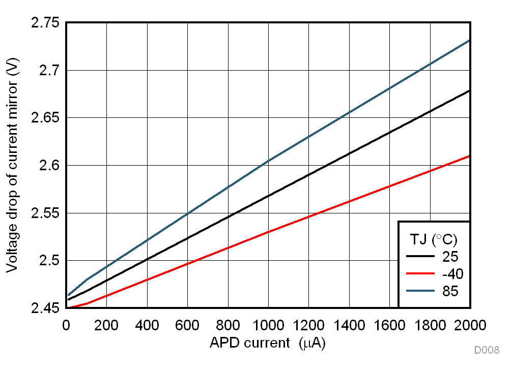
TPS61391 D008_SLVSEL7.gif
VIN = 3.3 V VOUT = 60 V
Figure 8. Voltage drop of current mirror vs. current