SLVSAW2C March 2012 – October 2016 TPS62090 , TPS62091 , TPS62092 , TPS62093
PRODUCTION DATA.
- 1 Features
- 2 Applications
- 3 Description
- 4 Revision History
- 5 Device Comparison Table
- 6 Pin Configuration and Functions
- 7 Specifications
-
8 Detailed Description
- 8.1 Overview
- 8.2 Functional Block Diagram
- 8.3
Feature Description
- 8.3.1 Enable and Disable (EN)
- 8.3.2 Softstart (SS) and Hiccup Current Limit During Startup
- 8.3.3 Voltage Tracking (SS)
- 8.3.4 Short Circuit Protection (Hiccup-Mode)
- 8.3.5 Output Discharge Function
- 8.3.6 Power Good Output (PG)
- 8.3.7 Frequency Set Pin (FREQ)
- 8.3.8 Undervoltage Lockout (UVLO)
- 8.3.9 Thermal Shutdown
- 8.3.10 Charge Pump (CP, CN)
- 8.4 Device Functional Modes
- 9 Application and Implementation
- 10Power Supply Recommendations
- 11Layout
- 12Device and Documentation Support
- 13Mechanical, Packaging, and Orderable Information
Package Options
Mechanical Data (Package|Pins)
- RGT|16
Thermal pad, mechanical data (Package|Pins)
- RGT|16
Orderable Information
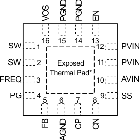
6 Pin Configuration and Functions
RGT Package
16-Pin QFN
Top View

NOTE:
*The exposed thermal pad is connected to AGND.Pin Functions
| PIN | I/O | DESCRIPTION | |
|---|---|---|---|
| NO. | NAME | ||
| 1, 2 | SW | I/O | Switch pin of the power stage. |
| 3 | FREQ | I | This pin selects the switching frequency of the device. FREQ = Low sets the typical switching frequency to 2.8 MHz. FREQ = High sets the typical switching frequency to 1.4 MHz. This pin has an active pull down resistor of typically 400 kΩ and can be left floating for 2.8 MHz operation. |
| 4 | PG | O | Power good open drain output. This pin is high impedance if the output voltage is within regulation. This pin is pulled low if the output is below its nominal value. The pull up resistor can not be connected to any voltage higher than the input voltage of the device. |
| 5 | FB | I | Feedback pin of the device. For the adjustable version, connect a resistor divider to set the output voltage. For the fixed output voltage versions this pin may be connected to GND for improved thermal performance and has a pull down resistor of typically 400 kΩ, which is active when EN is low. |
| 6 | AGND | Analog ground. | |
| 7 | CP | I/O | Internal charge pump flying capacitor. Connect a 10 nF capacitor between CP and CN. |
| 8 | CN | I/O | Internal charge pump flying capacitor. Connect a 10 nF capacitor between CP and CN. |
| 9 | SS | I | Softstart control pin. A capacitor is connected to this pin and sets the softstart time. Leaving this pin floating sets the minimum start-up time. |
| 10 | AVIN | I | Bias supply input voltage pin. |
| 11,12 | PVIN | I | Power supply input voltage pin. |
| 13 | EN | I | Device enable. To enable the device this pin needs to be pulled high. Pulling this pin low disables the device. This pin has a pull down resistor of typically 400 kΩ, which is active when EN is low. |
| 14,15 | PGND | Power ground connection. | |
| 16 | VOS | I | Output voltage sense pin. This pin needs to be connected to the output voltage. |
| Exposed Thermal Pad | – | The exposed thermal pad is connected to AGND. It must be soldered for mechanical reliability. | |