SLVSB35C October 2012 – July 2015 TPS62175 , TPS62177
PRODUCTION DATA.
- 1 Features
- 2 Applications
- 3 Description
- 4 Revision History
- 5 Device Comparison Table
- 6 Pin Configuration and Functions
- 7 Specifications
- 8 Detailed Description
-
9 Application and Implementation
- 9.1 Application Information
- 9.2 Typical Application
- 9.3 System Examples
- 10Power Supply Recommendations
- 11Layout
- 12Device and Documentation Support
- 13Mechanical, Packaging, and Orderable Information
Package Options
Refer to the PDF data sheet for device specific package drawings
Mechanical Data (Package|Pins)
- DQC|10
Thermal pad, mechanical data (Package|Pins)
Orderable Information
8 Detailed Description
8.1 Overview
The TPS6217x synchronous switch mode power converters are based on DCS-Control™ (Direct Control with Seamless Transition into Power Save Mode), an advanced regulation topology, that combines the advantages of hysteretic, voltage mode, and current mode control including an AC loop directly associated to the output voltage. This control loop takes information about output voltage changes and feeds it directly to a fast comparator stage. It sets the switching frequency, which is constant for steady state operating conditions, and provides immediate response to dynamic load changes. To get accurate DC load regulation, a voltage feedback loop is used. The internally compensated regulation network achieves fast and stable operation with small external components and low ESR capacitors. The DCS-Control topology supports pulse width modulation (PWM) mode for medium and heavy load conditions and a power save mode at light loads. During PWM, it operates at its nominal switching frequency in continuous conduction mode. This frequency is typically about 1 MHz with a controlled frequency variation depending on the input voltage. If the load current decreases, the converter enters power save mode to sustain high efficiency down to very light loads. In power save mode the switching frequency decreases linearly with the load current. Because DCS-Control™ supports both operation modes within one single building block, the transition from PWM to power save mode is seamless without effects on the output voltage. Fixed output voltage versions provide smallest solution size and lowest current consumption, requiring only 3 external components. An internal current limit supports nominal output currents of up to 500 mA. The TPS6217x offer both excellent DC voltage and superior load transient regulation, combined with very low output voltage ripple, minimizing interference with RF circuits.
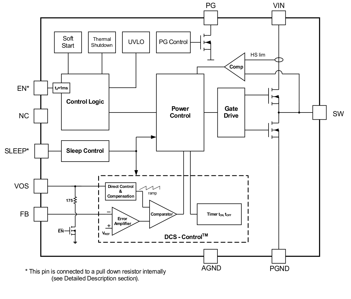
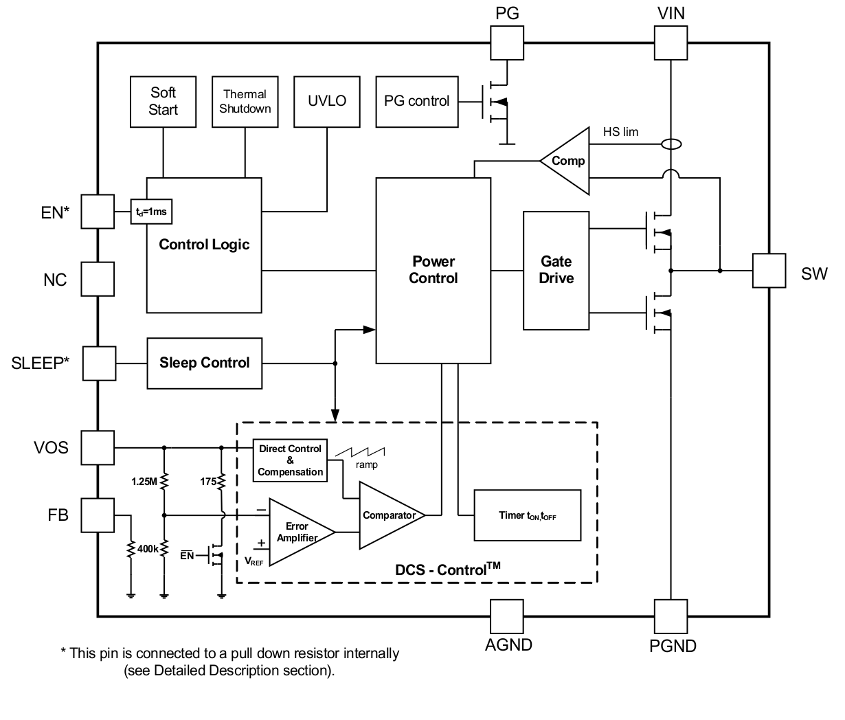
8.2 Functional Block Diagrams
 Figure 6. TPS62175 (Adjustable Output Voltage)
 Figure 7. TPS62177 (Fixed Output Voltage)
8.3 Feature Description
8.3.1 Enable/Shutdown (EN)
The device can be switched ON/OFF by pulling the EN pin to High (operation) or Low (shutdown). If EN is pulled to High, the device starts operation after a delay of about 1 ms (typical). This helps to ensure a monotonic start-up sequence, which makes the device ideally suited to control the power on sequence of micro controllers.
During shutdown, the internal MOSFETs as well as the entire control circuitry are turned off and the current consumption is typically 1.5 µA. The EN pin is connected through a 400-kΩ pulldown resistor, keeping the logic level low, if the pin is floating. The resistor is disconnected when EN is set High.
8.3.2 Output Discharge
The output is actively discharged through a 175-Ω (typical) resistor on the VOS pin when the device is turned off by EN, UVLO or thermal shutdown.
8.3.3 Current Limit and Short Circuit Protection
The TPS6217x devices are protected against heavy load and short circuit events. If a current limit situation is detected, the device switches off. The off-time is maintained longer as the output voltage becomes lower. At heavy overloads the low-side MOSFET stays on until the inductor current returns to zero. Then the high-side MOSFET turns on again (see Figure 50 and Figure 51).
8.3.4 Power Good (PG)
The TPS6217x has a built-in power good (PG) function to indicate that the output reached regulation. The PG signal can be used for start-up sequencing of multiple rails. The PG pin is an open-drain output that requires a pullup resistor (to any voltage less than 7 V). It can sink 2 mA of current and maintain its specified logic low level of 0.3 V. It is held low when the device is turned off by EN, UVLO or thermal shutdown.
If the PG pin is not used, it may be left floating or connected to AGND.
8.3.5 Undervoltage Lockout (UVLO)
If the input voltage drops, the undervoltage lockout function prevents misoperation by turning the device off. The undervoltage lockout threshold is set to 4.6 V (typically) for rising VIN. To cover for possible input voltage drops, when using high impedance sources or batteries, the falling threshold is set to typically 2.9 V, allowing monotonic start-up sequence under such conditions. For input voltages below the minimum VIN of 4.75 V and above the falling UVLO threshold of 2.9 V, the device still functions with a current limit and regulation capability but the electrical characteristics are no longer specified.
8.3.6 Thermal Shutdown
The junction temperature (TJ) of the device is monitored by an internal temperature sensor. If TJ exceeds 150°C (typical), the device goes into thermal shutdown. Both the high-side and low-side power FETs are turned off and PG goes Low. When TJ decreases below the hysteresis amount, the converter resumes normal operation, beginning with soft start. To avoid unstable conditions, a hysteresis of typically 20°C is implemented on the thermal shutdown temperature.
8.4 Device Functional Modes
8.4.1 Soft Start
The internal soft start circuitry controls the output voltage slope during start-up. This avoids excessive inrush current and ensures a controlled output voltage rise time. It also prevents unwanted voltage drops from high-impedance power sources or batteries. When EN is set to High and the device starts switching, VOUT rises with a slope of typically 10 mV/µs. The internal current limit is reduced to typically 525 mA during start-up. Thereby the output current is less than 500 mA during that time (see Figure 41). The start-up sequence ends when the device achieves regulation; then, the device runs with the full current limit of typically 1 A, providing full output current.
The TPS6217x can monotonically start into a prebiased output.
8.4.2 Pulse Width Modulation (PWM) Operation
The TPS6217x operates with pulse width modulation in continuous conduction mode (CCM) with a nominal switching frequency of about 1 MHz. The switching frequency in PWM is set by an internal timer circuit. The frequency variation is controlled and depends on VIN and VOUT. The device operates in PWM mode as long the output current is higher than half the inductor's ripple current. To maintain high efficiency at light loads, the device enters power save mode at the boundary to discontinuous conduction mode (DCM).
8.4.3 Power Save Mode Operation
The TPS6217x built in power save mode is entered seamlessly, if the load current decreases. This secures a high efficiency in light load operation by keeping the on-time fixed and reducing the switching frequency by incorporating pause time. The device remains in power save mode as long as the inductor current is discontinuous. The on-time, in steady-state PWM operation, can be estimated as:
spacing

spacing
In case Equation 1 yields a lower value, the device maintain an on-time of about 80 ns to limit switching losses. This minimum on-time is used in power save mode. While the peak inductor current in Power Save Mode can be approximated by:
spacing

spacing
The switching frequency is calculated as follows:
spacing

spacing
8.4.4 Sleep Mode Operation
In sleep mode operation, the typical quiescent current is reduced from 22 µA to 4.8 µA to significantly increase the efficiency at load currents of typically less than 1 mA (see Figure 1 and Figure 2). It is designed to be enabled and disabled during operation by pulling the SLEEP pin High or Low by the host (processor). Ultralow power micro controllers in deep sleep or hibernating mode may set their output pins floating. Therefore, the TPS6217x have a pulldown resistor internally connected to the SLEEP pin, to keep a logic low level, when the sleep input signal goes high impedance. But, if the sleep signal goes directly from logic High to High Impedance, the low level detection must be ensured considering the leakage of the micro controller's sleep signal. An external pulldown resistor, on the SLEEP pin, may be required. Connect the SLEEP pin to VOUT, not VIN, to disable sleep mode, because the pin's voltage rating is limited to 7 V maximum.
The output voltage is regulated with a fixed switching scheme, using a fixed on-time of about twice the minimum on-time of Equation 1 (compare Figure 48 and Figure 49) and the minimum off-time. A new pulse is initiated once the output voltage falls below its regulation threshold. Sleep mode is limited with its dynamic response and current capabilities. However, the device can deliver temporarily more than 15 mA while still in sleep mode, to allow micro controllers to wake up and drive the sleep signal High, exiting sleep mode.
Continuously operating with a too high current in sleep mode causes the output voltage to drop until the PG pin goes Low. As a safety feature, the device then returns to normal operation automatically, avoiding a complete collapse of VOUT. Once the load current decreases again, the device re-enters sleep mode operation. Certainly, this is not a recommended operation mode and sleep mode should be entered or exited by using the SLEEP pin logic.
Sleep mode is not entered until soft-start is complete.
8.4.5 100% Mode Operation
The duty cycle of the buck converter is given by D = VOUT/VIN and increases as the input voltage comes close to the output voltage. In this case, the device starts 100% duty cycle operation turning on the high-side switch 100% of the time. The high-side switch stays turned on as long as the output voltage is below the internal setpoint. This allows the conversion of small input to output voltage differences, for example, for longest operation time of battery-powered applications.
The minimum input voltage to maintain output voltage regulation can be calculated as:
spacing

where
- IOUT is the output current
- RDS(on) is the RDS(on) of the high-side FET
- RL is the DC resistance of the inductor used