SLVSB35C October 2012 – July 2015 TPS62175 , TPS62177
PRODUCTION DATA.
- 1 Features
- 2 Applications
- 3 Description
- 4 Revision History
- 5 Device Comparison Table
- 6 Pin Configuration and Functions
- 7 Specifications
- 8 Detailed Description
-
9 Application and Implementation
- 9.1 Application Information
- 9.2 Typical Application
- 9.3 System Examples
- 10Power Supply Recommendations
- 11Layout
- 12Device and Documentation Support
- 13Mechanical, Packaging, and Orderable Information
Package Options
Refer to the PDF data sheet for device specific package drawings
Mechanical Data (Package|Pins)
- DQC|10
Thermal pad, mechanical data (Package|Pins)
Orderable Information
11 Layout
11.1 Layout Guidelines
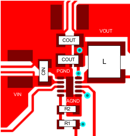
The input capacitor needs to be placed as close as possible to the IC pins (VIN, PGND). The inductor should be placed close to the SW pin and connect directly to the output capacitor - minimizing the loop area between the SW pin, inductor, output capacitor and PGND pin. Also, sensitive nodes like FB and VOS should be connected with short wires, not nearby high dv/dt signals (for example, SW). The feedback resistors, R1 and R2, should be placed close to the IC and connect directly to the AGND and FB pins.
A proper layout is critical for the operation of a switch mode power supply, even more at high switching frequencies. Therefore the PCB layout of the TPS6217x demands careful attention to ensure operation and to get the performance specified. A poor layout can lead to issues like poor regulation (both line and load), stability and accuracy weaknesses, increased EMI radiation and noise sensitivity. See Figure 62 for the recommended layout of the TPS62175, which is implemented on the EVM. Information can be found in the EVM Users Guide, TPS62175EVM-098 Evaluation Module (SLVU743). Alternatively, the EVM Gerber data are available for download here, SLVC453.
11.2 Layout Example
 Figure 62. Layout Example Recommendation
The exposed thermal pad must be soldered to AGND and on the circuit board for mechanical reliability and to achieve appropriate power dissipation.
11.3 Thermal Information
The TPS6217x is designed for a maximum operating junction temperature (TJ) of 125°C. Therefore the maximum output power is limited by the power losses. Because the thermal resistance of the package is given, the size of the surrounding copper area and a proper thermal connection of the IC can reduce the thermal resistance. To get an improved thermal behavior, TI recommends using top layer metal to connect the device with wide and thick metal lines (see Figure 62). Internal ground layers can connect to vias directly under the IC for improved thermal performance.
For more details on how to use the thermal parameters, see the application notes: Thermal Characteristics Application Note, Thermal Characteristics of Linear and Logic Packages Using JEDEC PCB Designs (SZZA017), and Semiconductor and IC Package Thermal Metrics (SPRA953).