SLVS417F March 2002 – June 2015 TPS62200 , TPS62201 , TPS62202 , TPS62203 , TPS62204 , TPS62205 , TPS62207 , TPS62208
PRODUCTION DATA.
- 1 Features
- 2 Applications
- 3 Description
- 4 Revision History
- 5 Pin Configuration and Functions
- 6 Specifications
- 7 Detailed Description
- 8 Application and Implementation
- 9 Power Supply Recommendations
- 10Layout
- 11Device and Documentation Support
- 12Mechanical, Packaging, and Orderable Information
Package Options
Refer to the PDF data sheet for device specific package drawings
Mechanical Data (Package|Pins)
- DBV|5
Thermal pad, mechanical data (Package|Pins)
Orderable Information
6 Specifications
6.1 Absolute Maximum Ratings
over operating free-air temperature range (unless otherwise noted) (1)| MIN | MAX | UNIT | ||
|---|---|---|---|---|
| VI | Supply voltages(2) | –0.3 | 7.0 | V |
| Voltages on pins SW, EN, FB (2) | –0.3 | VCC +0.3 | V | |
| PD | Continuous power dissipation | See Thermal Information | ||
| TJ | Operating junction temperature | –40 | 150 | °C |
| Tstg | Storage temperature | –65 | 150 | °C |
(1) Stresses beyond those listed under Absolute Maximum Ratings may cause permanent damage to the device. These are stress ratings only, which do not imply functional operation of the device at these or any other conditions beyond those indicated under Recommended Operating Conditions. Exposure to absolute-maximum-rated conditions for extended periods may affect device reliability.
(2) All voltage values are with respect to network ground terminal.
6.2 ESD Ratings
| VALUE | UNIT | |||
|---|---|---|---|---|
| V(ESD) | Electrostatic discharge | Human body model (HBM), per ANSI/ESDA/JEDEC JS-001(1) | ±2000 | V |
| Charged device model (CDM), per JEDEC specification JESD22-C101(2) | ±500 | |||
(1) JEDEC document JEP155 states that 500-V HBM allows safe manufacturing with a standard ESD control process.
(2) JEDEC document JEP157 states that 250-V CDM allows safe manufacturing with a standard ESD control process.
6.3 Recommended Operating Conditions
over operating free-air temperature range (unless otherwise noted)| MIN | NOM | MAX | UNIT | ||
|---|---|---|---|---|---|
| VI | Supply voltage | 2.5 | 6.0 | V | |
| VO | Output voltage for adjustable output voltage version | 0.7 | VI | V | |
| IO | Output current | 300 | mA | ||
| L | Inductor(1) | 4.7 | 10 | µH | |
| CI | Input capacitor(1) | 4.7 | µF | ||
| CO | Output capacitor(1) | 10 | µF | ||
| TA | Operating ambient temperature | 40 | 85 | °C | |
| TJ | Operating junction temperature | 40 | 125 | °C |
(1) See Application and Implementation for further information.
6.4 Thermal Information
| THERMAL METRIC(1) | TPS6220x | UNIT | |
|---|---|---|---|
| DBV [SOT-23] | |||
| 5 PINS | |||
| RθJA | Junction-to-ambient thermal resistance | 220 | °C/W |
| RθJC(top) | Junction-to-case (top) thermal resistance | 125 | °C/W |
| RθJB | Junction-to-board thermal resistance | 36 | °C/W |
| ψJT | Junction-to-top characterization parameter | 14 | °C/W |
| ψJB | Junction-to-board characterization parameter | 35 | °C/W |
| RθJC(bot) | Junction-to-case (bottom) thermal resistance | N/A | °C/W |
(1) For more information about traditional and new thermal metrics, see the Semiconductor and IC Package Thermal Metrics application report, SPRA953.
6.5 Electrical Characteristics
VI = 3.6 V, VO = 1.8 V, IO = 200 mA, EN = VIN, TA = –40°C to 85°C, typical values are at TA = 25°C (unless otherwise noted)| PARAMETER | TEST CONDITIONS | MIN | TYP | MAX | UNIT | ||
|---|---|---|---|---|---|---|---|
| SUPPLY CURRENT | |||||||
| VI | Input voltage | 2.5 | 6 | V | |||
| IQ | Operating quiescent current | IO = 0 mA, Device is not switching | 15 | 30 | µA | ||
| Shutdown supply current | EN = GND | 0.1 | 1 | µA | |||
| Undervoltage lockout threshold | 1.5 | 2 | V | ||||
| ENABLE | |||||||
| V(EN) | EN high level input voltage | 1.3 | V | ||||
| EN low level input voltage | 0.4 | V | |||||
| I(EN) | EN input bias current | EN = GND or VIN | 0.01 | 0.1 | µA | ||
| POWER SWITCH | |||||||
| rds(ON) | P-channel MOSFET on-resistance | VIN = VGS = 3.6 V | 530 | 690 | mΩ | ||
| VIN = VGS = 2.5 V | 670 | 850 | |||||
| N-channel MOSFET on-resistance | VIN = VGS = 3.6 V | 430 | 540 | mΩ | |||
| VIN = VGS = 2.5 V | 530 | 660 | |||||
| Ilkg_(P) | P-channel leakage current | VDS = 6.0 V | 0.1 | 1 | µA | ||
| Ilkg_(N) | N-channel leakage current | VDS = 6.0 V | 0.1 | 1 | µA | ||
| I(LIM) | P-channel current limit | 2.5 V < Vin < 6.0 V | 380 | 480 | 670 | mA | |
| OSCILLATOR | |||||||
| fS | Switching frequency | 650 | 1000 | 1500 | kHz | ||
| OUTPUT | |||||||
| VO | Adjustable output voltage | TPS62200 | 0.7 | VIN | V | ||
| Vref | Reference voltage | 0.5 | V | ||||
| Feedback voltage (1) | TPS62200 | VI = 3.6 V to 6 V, IO = 0 mA | 0% | 3% | |||
| Adjustable | VI = 3.6 V to 6 V, 0 mA ≤ IO ≤ 300 mA | –3% | 3% | ||||
| VO | Fixed output voltage(1) | TPS62207 | VI = 2.5 V to 6 V, IO = 0 mA | 0% | 3% | ||
| 1.2 V | VI = 2.5 V to 6 V, 0 mA ≤ IO ≤ 300 mA | –3% | 3% | ||||
| TPS62201 | VI = 2.5 V to 6 V, IO = 0 mA | 0% | 3% | ||||
| 1.5 V | VI = 2.5 V to 6 V, 0 mA ≤ IO ≤ 300 mA | –3% | 3% | ||||
| TPS62204 | VI = 2.5 V to 6 V, IO = 0 mA | 0% | 3% | ||||
| 1.6 V | VI = 2.5 V to 6 V, 0 mA ≤ IO ≤ 300 mA | –3% | 3% | ||||
| TPS62202 | VI = 2.5 V to 6 V, IO = 0 mA | 0% | 3% | ||||
| 1.8 V | VI = 2.5 V to 6 V, 0 mA ≤ IO ≤ 300 mA | –3% | 3% | ||||
| TPS62208 | VI = 2.5 V to 6 V, IO = 0 mA | 0% | 3% | ||||
| 1.875 V | VI = 2.5 V to 6 V, 0 mA ≤ IO ≤ 300 mA | –3% | 3% | ||||
| TPS62205 | VI = 2.7 V to 6 V, IO = 0 mA | 0% | 3% | ||||
| 2.5 V | VI = 2.7 V to 6 V, 0 mA ≤ IO ≤ 300 mA | –3% | 3% | ||||
| TPS62203 | VI = 3.6 V to 6 V, IO = 0 mA | 0% | 3% | ||||
| 3.3 V | VI = 3.6 V to 6 V, 0 mA ≤ IO ≤ 300 mA | –3% | 3% | ||||
| Line regulation | VI = 2.5 V to 6 V, IO = 10 mA | 0.26 | %/V | ||||
| Load regulation | IO = 100 mA to 300 mA | 0.0014 | %/mA | ||||
| Ilkg | Leakage current into SW pin | Vin > Vout, 0 V ≤ Vsw ≤ Vin | 0.1 | 1 | µA | ||
| Ilkg(Rev) | Reverse leakage current into pin SW | Vin = open, EN = GND, VSW = 6 V | 0.1 | 1 | µA | ||
(1) For output voltages ≤ 1.2 V, a 22-µF output capacitor value is required to achieve a maximum output voltage accuracy of 3% while operating in power save mode (PFM mode).
6.6 Typical Characteristics
Table 1. Table of Graphs
| FIGURES | |||
|---|---|---|---|
| η | Efficiency | vs Load current | Figure 6, Figure 7, Figure 8 |
| vs Input voltage | Figure 9 | ||
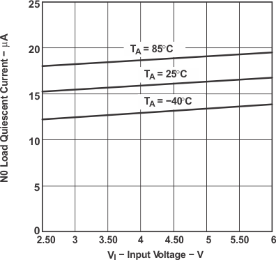
| IQ | No load quiescent current | vs Input voltage | Figure 1 |
| fs | Switching frequency | vs Temperature | Figure 10 |
| Vo | Output voltage | vs Output current | Figure 11 |
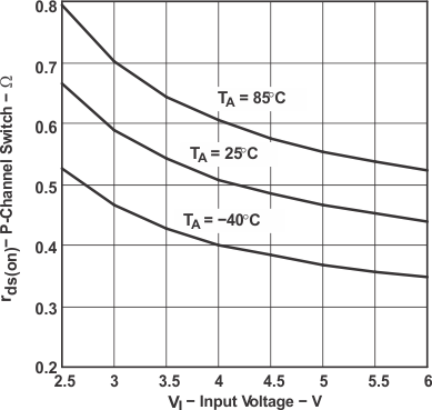
| rds(on) | rds(on) - P-channel switch, | vs Input voltage | Figure 2 |
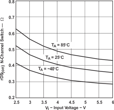
| rds(on) - N-channel rectifier switch | vs Input voltage | Figure 3 | |
| Line transient response | Figure 12 | ||
| Load transient response | Figure 13 | ||
| Power save mode operation | Figure 14 | ||
| Start-up | Figure 15 | ||


