SLVS762C June 2007 – July 2015 TPS62240 , TPS62242 , TPS62243
PRODUCTION DATA.
- 1 Features
- 2 Applications
- 3 Description
- 4 Revision History
- 5 Device Options
- 6 Pin Configuration and Functions
- 7 Specifications
- 8 Detailed Description
- 9 Application and Implementation
- 10Power Supply Recommendations
- 11Layout
- 12Device and Documentation Support
- 13Mechanical, Packaging, and Orderable Information
Package Options
Mechanical Data (Package|Pins)
Thermal pad, mechanical data (Package|Pins)
- DRV|6
Orderable Information
6 Pin Configuration and Functions
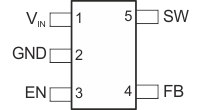
DDC Package
5-Pin SOT
Top View

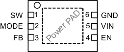
DRV Package
6-Pin WSON
Top View

Pin Functions
| PIN | I/O | DESCRIPTION | ||
|---|---|---|---|---|
| NAME | WSON | SOT | ||
| EN | 4 | 3 | I | This is the enable pin of the device. Pulling this pin to low forces the device into shutdown mode. Pulling this pin to high enables the device. This pin must be terminated. |
| GND | 6 | 2 | PWR | GND supply pin. |
| FB | 3 | 4 | I | Feedback pin for the internal regulation loop. Connect the external resistor divider to this pin. In case of fixed output voltage option, connect this pin directly to the output capacitor. |
| MODE | 2 | — | I | This pin is only available at WSON package option. MODE pin = High forces the device to operate in fixed-frequency PWM mode. MODE pin = Low enables the power save mode with automatic transition from PFM mode to fixed-frequency PWM mode. |
| SW | 1 | 5 | O | This is the switch pin and is connected to the internal MOSFET switches. Connect the inductor to this terminal. |
| VIN | 5 | 1 | PWR | VIN power supply pin. |