SLVSBO4C October 2012 – December 2014 TPS62736 , TPS62737
UNLESS OTHERWISE NOTED, this document contains PRODUCTION DATA.
- 1 Features
- 2 Applications
- 3 Description
- 4 Revision History
- 5 Description (continued)
- 6 Device Voltage Options
- 7 Pin Configuration and Functions
- 8 Specifications
- 9 Detailed Description
- 10Application and Implementation
- 11Power Supply Recommendations
- 12Layout
- 13Device and Documentation Support
- 14Mechanical, Packaging, and Orderable Information
Package Options
Mechanical Data (Package|Pins)
- RGY|14
Thermal pad, mechanical data (Package|Pins)
- RGY|14
Orderable Information
12 Layout
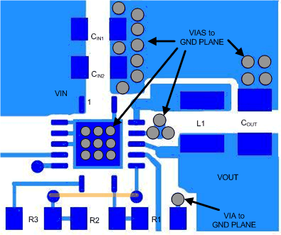
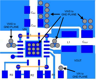
12.1 Layout Guidelines
To minimize switching noise generation, the step-down converter (buck) power stage external components must be carefully placed. The most critical external component for a buck power stage is its input capacitor. The bulk input capacitor (CIN1) and high frequency decoupling capacitor (CIN2) must be placed as close as possible between the power stage input (IN pin 1) and ground (VSS pin 12). Next, the inductor (L1) must be placed as close as possible beween the switching node (SW pin 13) and the output voltage (OUT pin 11). Finally, the output capacitor (COUT) should be placed as close as possible between the output voltage (OUT pin 11) and GND (VSS pin 12). In the diagram below, the input and output capacitor grounds are connected to VSS pin 12 through vias to the bottom-layer ground plane of the PCB.
To minimize noise pickup by the high impedance voltage setting nodes (VIN_OK_SET pin 8 and VOUT_SET pin 9), the external resistors (R1, R2 and R3) should be placed so that the traces connecting the midpoints of the string are as short as possible. In the diagram below, the connection to VOUT_SET is by a bottom layer trace.
The remaining pins are either NC pins, that should be connected to the PowerPAD™ as shown below, or digital signals with minimal layout restrictions.
In order to maximize efficiency at light load, the use of voltage level setting resistors > 1 MΩ is recommended. However, during board assembly, contaminants such as solder flux and even some board cleaning agents can leave residue that may form parasitic resistors across the physical resistors and/or from one end of a resistor to ground, especially in humid, fast airflow environments. This can result in the voltage regulation and threshold levels changing significantly from those expected per the installed resistor values. Therefore, it is highly recommended that no ground planes be poured near the voltage setting resistors. In addition, the boards must be carefully cleaned, possibly rotated at least once during cleaning, and then rinsed with de-ionized water until the ionic contamination of that water is well above 50 MΩ. If this is not feasible, then it is recommended that the sum of the voltage setting resistors be reduced to at least 5 times below the measured ionic contamination.