SLVSB02B November 2013 – July 2014 TPS62740 , TPS62742
PRODUCTION DATA.
- 1 Features
- 2 Applications
- 3 Description
- 4 Revision History
- 5 Device Comparison Table
- 6 Specifications
- 7 Detailed Description
- 8 Application and Implementation
- 9 Power Supply Recommendations
- 10Layout
- 11Device and Documentation Support
- 12Mechanical, Packaging, and Orderable Information
Package Options
Mechanical Data (Package|Pins)
- DSS|12
Thermal pad, mechanical data (Package|Pins)
- DSS|12
Orderable Information
7 Detailed Description
7.1 Overview
The TPS6274x is the first step down converter with an ultra low quiescent current consumption (360nA typ.) and featuring TI's DCS-Control™ topology while maintaining a regulated output voltage. The device extends high efficiency operation to output currents down to a few micro amperes.
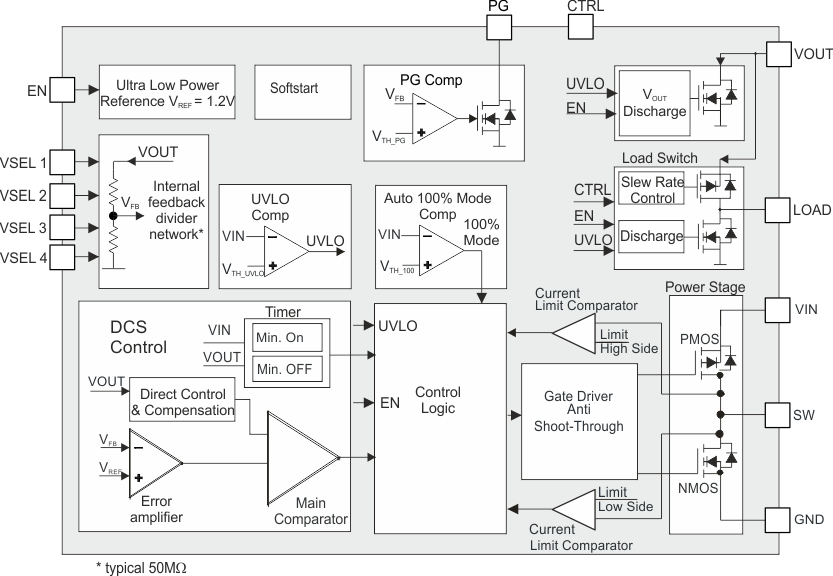
7.2 Functional Block Diagram
7.3 Feature Description
7.3.1 DCS-Control™
TI's DCS-Control™ (Direct Control with Seamless Transition into Power Save Mode) is an advanced regulation topology, which combines the advantages of hysteretic and voltage mode control. Characteristics of DCS-Control™ are excellent AC load regulation and transient response, low output ripple voltage and a seamless transition between PFM and PWM mode operation. DCS-Control™ includes an AC loop which senses the output voltage (VOUT pin) and directly feeds the information to a fast comparator stage. This comparator sets the switching frequency, which is constant for steady state operating conditions, and provides immediate response to dynamic load changes. In order to achieve accurate DC load regulation, a voltage feedback loop is used. The internally compensated regulation network achieves fast and stable operation with small external components and low ESR capacitors.
The DCS-Control™ topology supports PWM (Pulse Width Modulation) mode for medium and high load conditions and a Power Save Mode at light loads. During PWM mode, it operates in continuous conduction. The switching frequency is up to 2MHz with a controlled frequency variation depending on the input voltage. If the load current decreases, the converter seamlessly enters Power Save Mode to maintain high efficiency down to very light loads. In Power Save Mode the switching frequency varies nearly linearly with the load current. Since DCS-Control™ supports both operation modes within one single building block, the transition from PWM to Power Save Mode is seamless without effects on the output voltage. The TPS6274x offers both excellent DC voltage and superior load transient regulation, combined with very low output voltage ripple, minimizing interference with RF circuits. At high load currents, the converter operates in quasi fixed frequency PWM mode operation and at light loads, in PFM (Pulse Frequency Modulation) mode to maintain highest efficiency over the full load current range. In PFM Mode, the device generates a single switching pulse to ramp up the inductor current and recharge the output capacitor, followed by a sleep period where most of the internal circuits are shutdown to achieve a lowest quiescent current. During this time, the load current is supported by the output capacitor. The duration of the sleep period depends on the load current and the inductor peak current.
During the sleep periods, the current consumption of TPS6274x is reduced to 360nA. This low quiescent current consumption is achieved by an ultra low power voltage reference, an integrated high impedance (typ. 50MΩ) feedback divider network and an optimized DCS-Control™ block.
7.3.2 CTRL / Output Load
With the CTRL pin set to high, the LOAD pin is connected to the VOUT pin via an load switch and can power up an additional, temporarily used sub-system. The load switch is slew rate controlled to support soft switching and not to impact the regulated output VOUT. If CTRL pin is pulled to GND, the LOAD pin is disconnected from the VOUT pin and internally connected to GND by an internal discharge switch. When CTRL pin is set to high, the Quiescent current of the DCS control block is increased to typ. 12.5µA. This ensures excellent transient response on both outputs VOUT and LOAD in case of a sudden load step at the LOAD output. The CTRL pin can be controlled by a micro controller.
7.3.3 Enable / Shutdown
The DC/DC converter is activated when the EN pin is set to high. For proper operation, the pin must be terminated and must not be left floating. With the EN pin set to low, the device enters shutdown mode with less than typ. 70nA current consumption.
7.3.4 Power Good Output (PG)
The Power Good comparator features an open drain output. The PG comparator is active with EN pin set to high and VIN is above the threshold VTH_UVLO+. It is driven to high impedance once VOUT trips the threshold VTH_PG+ for rising VOUT. The output is pulled to low level once VOUT falls below the PG hysteresis, VPG_hys. The output is also pulled to low level in case the input voltage VIN falls below the undervoltage lockout threshold VTH_UVLO- or the device is disabled with EN = low. The power good output (PG) can be used as an indicator for the system to signal that the converter has started up and the output voltage is in regulation.
7.3.5 Output Voltage Selection (VSEL1 – 4)
The TPS6274x doesn't require an external resistor divider network to program the output voltage. The device integrates a high impedance (typ. 50MΩ) feedback resistor divider network which is programmed by the pins VSEL 1-4. TPS6274x supports an output voltage range of 1.8V to 3.3V in 100mV steps. The output voltage can be changed during operation and supports a simple dynamic output voltage scaling, shown in . The output voltage is programmed according to table Table 1.
7.3.6 Softstart
When the device is enabled, the internal reference is powered up and after the startup delay time tStartup_delay has expired, the device enters softstart, starts switching and ramps up the output voltage. During softstart the device operates with a reduced current limit, ILIM_softstart, of typ. 1/4 of the nominal current limit. This reduced current limit is active during the softstart time tSoftstart. The current limit is increased to its nominal value, ILIMF, once the softstart time has expired.
7.3.7 Undervoltage Lockout UVLO
The device includes an under-voltage lockout (UVLO) comparator which prevents the device from misoperation at too low input voltages. The UVLO comparator becomes active once the device is enabled with EN set to high. Once the input voltage trips the UVLO threshold VTH_UVLO+ (typically 2.075V) for rising VIN, the UVLO comparator releases the device for start up and operation. With a falling input voltage, the device operates down to the UVLO threshold level VTH_UVLO- (typically 1.925V). Once this threshold is tripped, the device stops switching, the load switch at pin LOAD is disabled and both rails, VOUT and LOAD are discharged. The converter starts operation again once the input voltage trips the rising UVLO threshold level VTH_UVLO+.
7.4 Device Functional Modes
7.4.1 VOUT And LOAD Output Discharge
Both the VOUT pin and the LOAD pin feature a discharge circuit to connect each rail to GND, once they are disabled. This feature prevents residual charge voltages on capacitors connected to these pins, which may impact proper power up of the main- and sub-system. With CTRL pin pulled to low, the discharge circuit at the LOAD pin becomes active. With the EN pin pulled to low, the discharge circuits at both pins VOUT and Load are active. The discharge circuits of both rails VOUT and LOAD are associated with the UVLO comparator as well. Both discharge circuits become active once the UVLO comparator triggers and the input voltage VIN has dropped below the UVLO comparator threshold VTH_UVLO- (typ. 1.925V).
7.4.2 Automatic Transition Into 100% Mode
Once the input voltage comes close to the output voltage, the DC/DC converter stops switching and enters 100% duty cycle operation. It connects the output VOUT via the inductor and the internal high side MOSFET switch to the input VIN, once the input voltage VIN falls below the 100% mode enter threshold, VTH_100-. The DC/DC regulator is turned off, not switching and therefore it generates no output ripple voltage. Because the output is connected to the input, the output voltage tracks the input voltage minus the voltage drop across the internal high side switch and the inductor caused by the output current. Once the input voltage increases and trips the 100% mode leave threshold, VTH_100+ , the DC/DC regulator turns on and starts switching again. See Figure 6, , , .
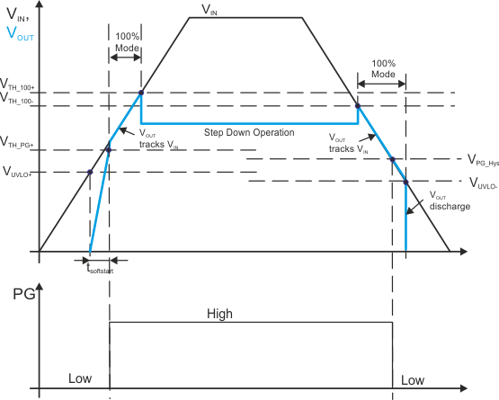 Figure 6. Automatic 100% Mode Transition
7.4.3 Internal Current Limit
The TPS6274x integrates a current limit on the high side, as well the low side MOSFETs to protect the device against overload or short circuit conditions. The peak current in the switches is monitored cycle by cycle. If the high side MOSFET current limit is reached, the high side MOSFET is turned off and the low side MOSFET is turned on until the current decreases below the low side MOSFET current limit.