SLVSB02B November 2013 – July 2014 TPS62740 , TPS62742
PRODUCTION DATA.
- 1 Features
- 2 Applications
- 3 Description
- 4 Revision History
- 5 Device Comparison Table
- 6 Specifications
- 7 Detailed Description
- 8 Application and Implementation
- 9 Power Supply Recommendations
- 10Layout
- 11Device and Documentation Support
- 12Mechanical, Packaging, and Orderable Information
Package Options
Mechanical Data (Package|Pins)
- DSS|12
Thermal pad, mechanical data (Package|Pins)
- DSS|12
Orderable Information
8 Application and Implementation
8.1 Application Information
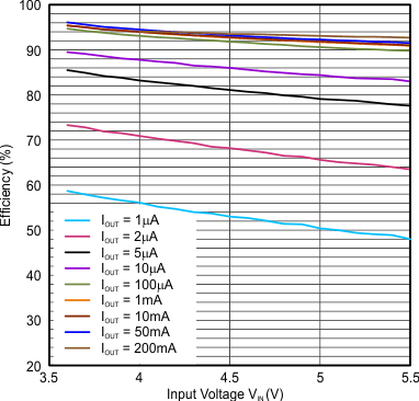
The TPS6274x devices are a step down converter family featuring typ. 360nA quiescent current and operating with a tiny 2.2µH inductor and 10µF output capacitor. This new DCS-ControlTM based devices extend the light load efficiency range below 10µA load currents. TPS62740 supports output currents up to 300mA, TPS62742 up to 400mA. The devices operate from rechargeable Li-Ion batteries, Li-primary battery chemistries such as Li-SOCl2, Li-MnO2 and two or three cell alkaline batteries.
8.2 Typical Application
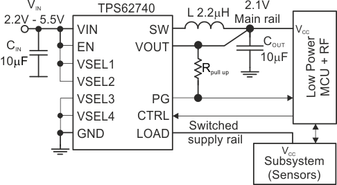 Figure 7. TPS62740 Typical Application Circuit
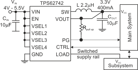 Figure 8. TPS62742 Typical Application Circuit
8.2.1 Design Requirements
The TPS6274x is a highly integrated DC/DC converter. The output voltage is set via a VSEL pin interface without any additional external components. For proper operation only a input- and output capacitor and an inductor is required. The integrated load switch doesn't require a capacitor on its LOAD pin. Table 2 shows the components used for the application characteristic curves.
Table 2. Components for Application Characteristic Curves
| Reference | Description | Value | Manufacturer |
|---|---|---|---|
| TPS62740/42 | 360nA Iq step down converter | Texas Instruments | |
| CIN, COUT, CLOAD | Ceramic capacitor GRM188R60J106M | 10µF | Murata |
| L | Inductor LPS3314 | 2.2µH | Coilcraft |
Detailed Design Procedure
Table 3 shows the recommended output filter components. The TPS6274x is optimized for operation with a 2.2µH inductor and with 10µF output capacitor.
Table 3. Recommended LC Output Filter Combinations
| Inductor Value [µH](2) | Output Capacitor Value [µF](1) | ||
|---|---|---|---|
| 4.7µF | 10µF | 22µF | |
| 2.2 | √ | √(3) | √ |
8.2.1.1 Inductor Selection
The inductor value affects its peak-to-peak ripple current, the PWM-to-PFM transition point, the output voltage ripple and the efficiency. The selected inductor has to be rated for its DC resistance and saturation current. The inductor ripple current (ΔIL) decreases with higher inductance and increases with higher VIN or VOUT and can be estimated according to Equation 1.
Equation 2 calculates the maximum inductor current under static load conditions. The saturation current of the inductor should be rated higher than the maximum inductor current, as calculated with Equation 2. This is recommended because during a heavy load transient the inductor current rises above the calculated value. A more conservative way is to select the inductor saturation current above the high-side MOSFET switch current limit, ILIMF.
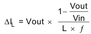
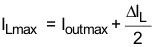
With:
f = Switching Frequency
L = Inductor Value
ΔIL= Peak to Peak inductor ripple current
ILmax = Maximum Inductor current
In DC/DC converter applications, the efficiency is essentially affected by the inductor AC resistance (i.e. quality factor) and by the inductor DCR value. Increasing the inductor value produces lower RMS currents, but degrades transient response. For a given physical inductor size, increased inductance usually results in an inductor with lower saturation current.
The total losses of the coil consist of both the losses in the DC resistance (RDC) and the following frequency-dependent components:
- The losses in the core material (magnetic hysteresis loss, especially at high switching frequencies)
- Additional losses in the conductor from the skin effect (current displacement at high frequencies)
- Magnetic field losses of the neighboring windings (proximity effect)
- Radiation losses
The following inductor series from different suppliers have been used:
Table 4. List Of Inductors(1)
| INDUCTANCE [µH] | DIMENSIONS [mm3] | INDUCTOR TYPE | SUPPLIER | |
|---|---|---|---|---|
| 2.2 | 3.3 x 3.3 x 1.4 | LPS3314 | Coilcraft | |
| 2.2 | 2.5 x 3.0 x 1.5 | VLF302515MT | TDK | |
| 2.2 | 2.0 × 1.2 × 1.0 | MIPSZ2012 2R2 | FDK | |
| 2.2 | 2.5 x 2.0 x 1.2 | MIPSA2520 2R2 | FDK | |
| 2.2 | 2.0 x 1.2 x 1.0 | MDT2012CH2R2 | TOKO | |
8.2.1.2 DC/DC Output Capacitor Selection
The DCS-Control™ scheme of the TPS6274x allows the use of tiny ceramic capacitors. Ceramic capacitors with low ESR values have the lowest output voltage ripple and are recommended. The output capacitor requires either an X7R or X5R dielectric. Y5V and Z5U dielectric capacitors, aside from their wide variation in capacitance over temperature, become resistive at high frequencies. At light load currents, the converter operates in Power Save Mode and the output voltage ripple is dependent on the output capacitor value and the PFM peak inductor current. A larger output capacitors can be used, but it should be considered that larger output capacitors lead to an increased leakage current in the capacitor and may reduce overall conversion efficiency. Furthermore, larger output capacitors impact the start up behavior of the DC/DC converter.
8.2.1.3 Input Capacitor Selection
Because the buck converter has a pulsating input current, a low ESR input capacitor is required for best input voltage filtering to ensure proper function of the device and to minimize input voltage spikes. For most applications a 10µF is sufficient. The input capacitor can be increased without any limit for better input voltage filtering.
Table 5 shows a list of tested input/output capacitors.
Table 5. List Of Capacitors(1)
| CAPACITANCE [μF] | SIZE | CAPACITOR TYPE | SUPPLIER |
|---|---|---|---|
| 10 | 0603 | GRM188R60J106ME84 | Murata |
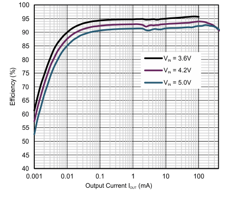
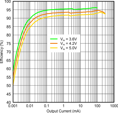
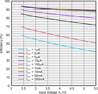
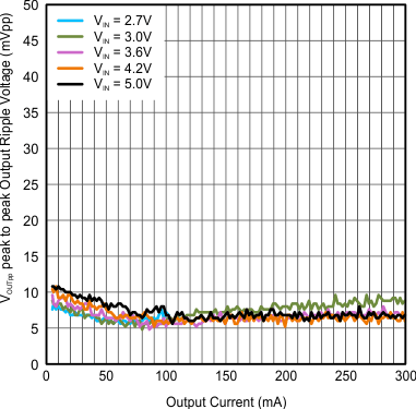
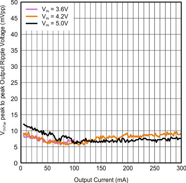
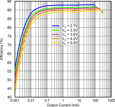
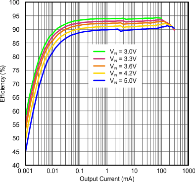
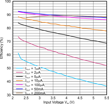
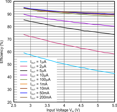
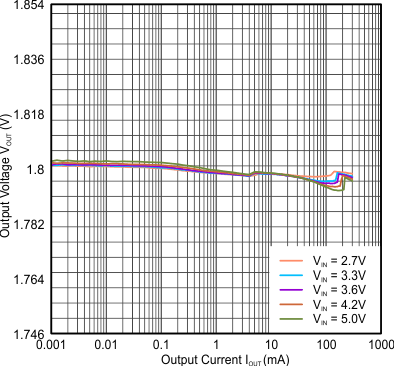
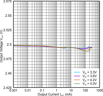
8.2.2 Application Curves
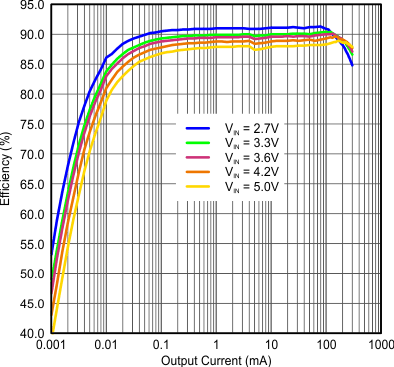
| COUT = 10 µF (0603) | CTRL = GND | |
| L = 2.2 µH (LPS3314 2R2) | ||
| COUT = 10 µF (0603) | CTRL = GND | |
| L = 2.2 µH (LPS3314 2R2) | ||
| COUT = 10 µF (0603) | CTRL = GND | |
| L = 2.2 µH (LPS3314 2R2) | ||
| COUT = 10 µF (0603) | CTRL = GND | |
| L = 2.2 µH (LPS3314 2R2) | ||
| COUT = 10 µF (0603) | CTRL = GND | |
| L = 2.2 µH (LPS3314 2R2) | ||
| COUT = 10 µF (0603) | CTRL = GND | |
| L = 2.2 µH (LPS3314 2R2) | ||
| COUT = 10 µF (0603) | CTRL = GND | |
| L = 2.2 µH | ||
| COUT = 10 µF (0603) | CTRL = GND | |
| L = 2.2 µH | ||
| COUT = 10 µF (0603) | CTRL = GND | |
| L = 2.2 µH |
| L = 2.2 µH (LPS3314) | ||
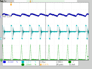
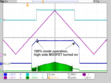
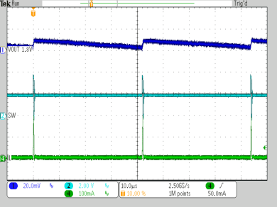
| VIN = 3.6 V | IOUT = 10 µA | L = 2.2 µH |
| COUT = 10 µF | CTRL = GND |
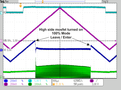
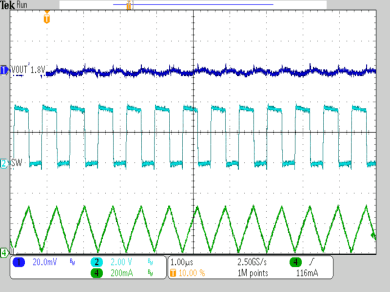
| VIN = 3.6 V | IOUT = 25 mA | L = 2.2 µH |
| COUT = 10 µF | CTRL = GND |
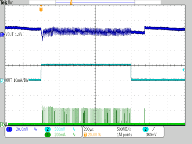
| VIN = 3.6 V | IOUT = 50 µA to 10 mA | L = 2.2 µH |
| COUT = 10 µF | CTRL = GND |
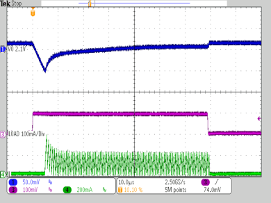
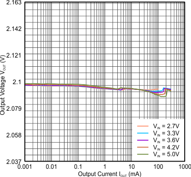
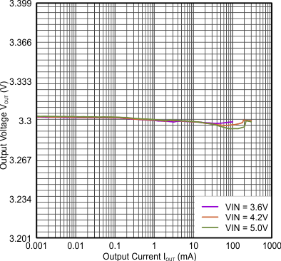
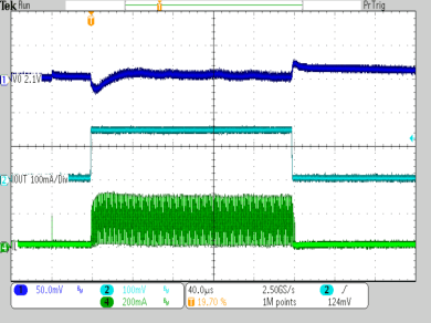
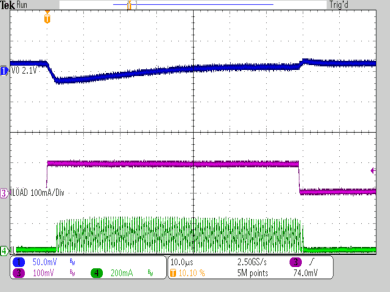
| VIN = 3.6 V, VOUT = 2.1 V | L = 2.2 µH | COUT = 10 µF |
| Loadstep at VOUT 0 mA to 100 mA, | ||
| 1 µs rise/ fall time, 70 µs / 7 ms | ||
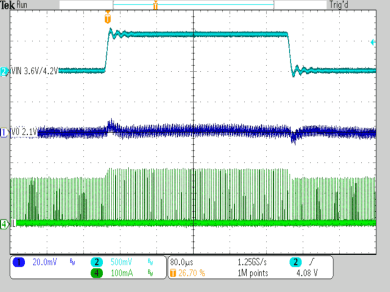
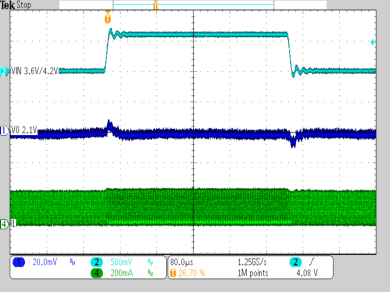
| VIN = 3.6 V / 4.2 V | VOUT = 2.1 V | L = 2.2 µH |
| COUT = 10 µF | CTRL = GND |
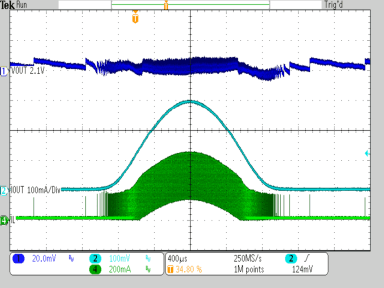
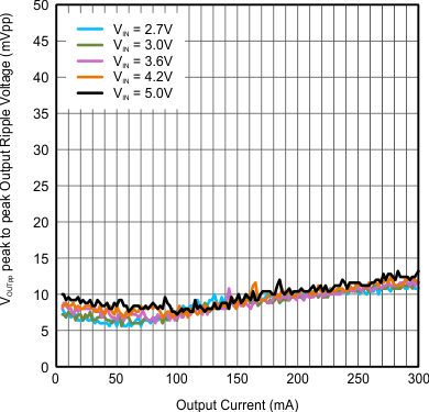
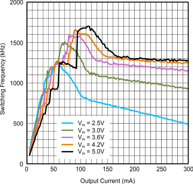
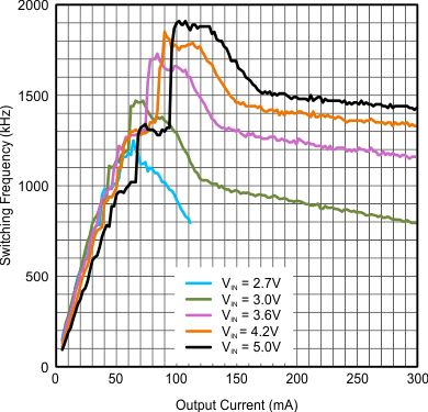
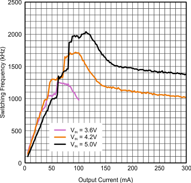
| VIN = 3.6 V | IOUT = 50 µA to 300 mA | L = 2.2 µH |
| COUT = 10 µF | CTRL = GND | |
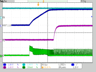
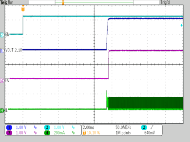
| VIN = 3.6 V | VOUT = 2.1 V | ILOAD = 0 mA |
| IOUT = 0 mA | COUT = 10 µF | CLOAD = 10 µF |
| L = 2.2 µH |
| VIN = 3.6 V | VOUT = 2.1 V | CTRL = GND |
| ROUT = 100 Ω | COUT = 10 µF | L = 2.2 µH |
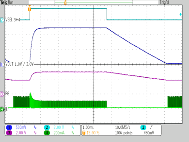
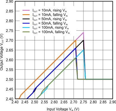
| VIN = 3.6 V | Ramp up / Down | |
| COUT = 10 µF | CTRL = GND | VSEL 3+4 toggled |
| IOUT = 5 mA | L = 2.2 µH | VSEL 1+2 = GND |
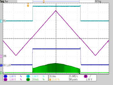
VOUT = 1.8V/3.0V
| COUT = 10 µF | L = 2.2 µH | CTRL = GND | |
| VIN = ramp up/down 0 V to 5 V, 150 ms, | |||
| Output resistance 50 Ω | |||
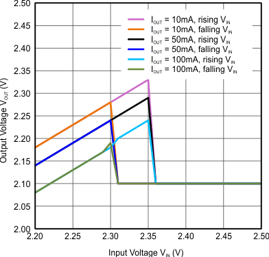
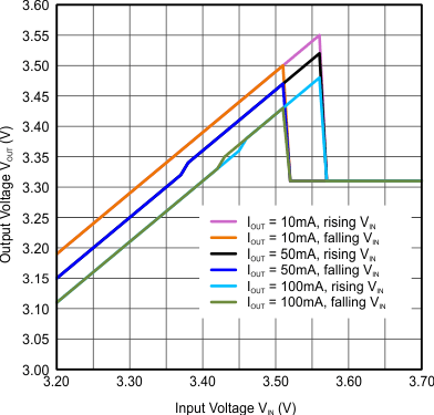
| VOUT = 3.0 V | COUT = 10 µF | L = 2.2 µH, CTRL = GND | ||
| VIN = ramp up /down 2.8 V to 3.7 V, | ||||
| Output resistance 50 Ω | ||||
| COUT = 10 µF (0603) | CTRL = GND | |
| L = 2.2 μH (LPS3314 2R2) | ||
| COUT = 10 µF (0603) | CTRL = GND | |
| L = 2.2 µH (LPS3314 2R2) | ||
| COUT = 10 µF (0603) | CTRL = GND | |
| L = 2.2 µH (LPS3314 2R2) | ||
| COUT = 10 µF (0603) | CTRL = GND | |
| L = 2.2 µH (LPS3314 2R2) | ||
| COUT = 10 µF (0603) | CTRL = GND | |
| L = 2.2 µH (LPS3314 2R2) | ||
| COUT = 10 µF (0603) | CTRL = GND | |
| L = 2.2 µH (LPS3314 2R2) | ||
| COUT = 10 µF | L = 2.2 µH | |
| COUT = 10 µF | L = 2.2 µH | |
| COUT = 10 µF | L = 2.2 µH | |
| L = 2.2 µH (LPS3314) | ||
| L = 2.2 µH (LPS3314) | ||
| VIN = 3.6 V | IOUT = 1 mA | L = 2.2 µH | |
| COUT = 10 µF | CTRL = GND | ||
| VIN = 3.6 V | IOUT = 150 mA | L = 2.2 µH |
| COUT = 10 µF | CTRL = GND |
| VIN = 3.6 V | IOUT = 0.5 mA to 150 mA | L = 2.2 µH |
| COUT = 10 µF | CTRL = VIN |
| VIN = 3.6 V, VOUT = 2.1 V | L = 2.2 µH, | COUT = 10 µF |
| Loadstep at VOUT 0 mA to 100 mA, | ||
| 1 µs rise/fall time; 70 µs / 7 ms | ||
| VIN = 3.6 V / 4.2 V | VOUT = 2.1 V | L = 2.2 µH |
| COUT = 10 µF | CTRL = GND |
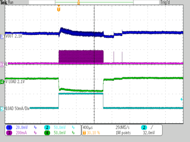
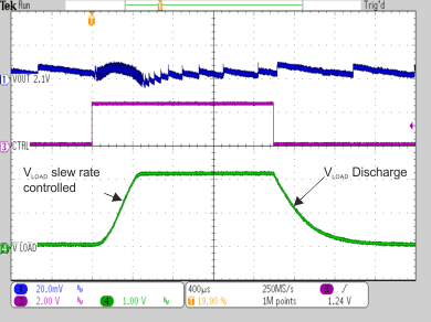
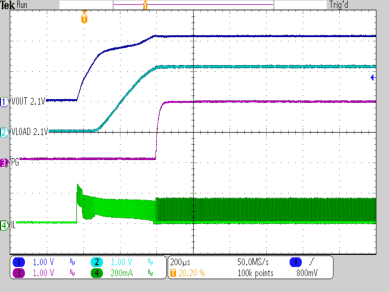
| VIN = 3.6 V, | VOUT = VLOAD= 2.1 V | CTRL = VIN | |
| IOUT = 0 mA | CLOAD = 10 µF | L = 2.2 µH | |
| COUT = 10 µF | ILOAD = 0 to 50 mA to 0 mA | ||
| VIN = 3.6 V | VOUT = 2.1 V | CTRL = GND |
| ROUT = 100 Ω | COUT = 10 µF | L = 2.2 µH |
| VIN = 3.6 V | VOUT = VLOAD = 2.1 V | CTRL = VIN |
| ROUT = 100 Ω, | COUT = CLOAD = 10 µF | L = 2.2 µH |
| ILOAD = 0 mA |
| COUT = 10 µF | L = 2.2 µH | CTRL = GND | ||
| VIN = ramp up/down 0 V to 5 V, 150 ms, | ||||
| Output resistance 50 Ω | ||||
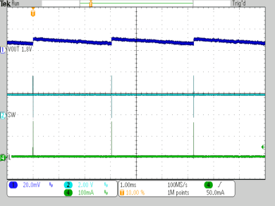
VOUT = 1.8V
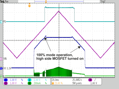
| COUT = 10 µF | L = 2.2 µH | CTRL = GND | ||
| VIN = ramp up/down 0 V to 5 V, 150 ms, | ||||
| Output resistance 50 Ω | ||||
8.3 System Example
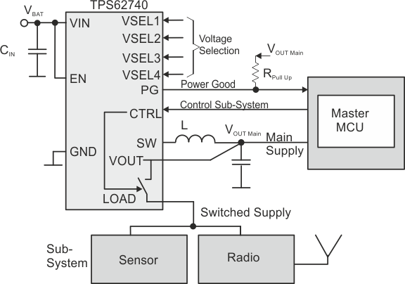 Figure 42. Example Of Implementation In A Master MCU Based System