SLVSB02B November 2013 – July 2014 TPS62740 , TPS62742
PRODUCTION DATA.
- 1 Features
- 2 Applications
- 3 Description
- 4 Revision History
- 5 Device Comparison Table
- 6 Specifications
- 7 Detailed Description
- 8 Application and Implementation
- 9 Power Supply Recommendations
- 10Layout
- 11Device and Documentation Support
- 12Mechanical, Packaging, and Orderable Information
Package Options
Mechanical Data (Package|Pins)
- DSS|12
Thermal pad, mechanical data (Package|Pins)
- DSS|12
Orderable Information
10 Layout
10.1 Layout Guidelines
As for all switching power supplies, the layout is an important step in the design. Care must be taken in board layout to get the specified performance. If the layout is not carefully done, the regulator could show poor line and/or load regulation, stability issues as well as EMI problems and interference with RF circuits. It is critical to provide a low inductance, impedance ground path. Therefore, use wide and short traces for the main current paths. The input capacitor should be placed as close as possible to the IC pins VIN and GND. The output capacitor should be placed close between VOUT and GND pins. The VOUT line should be connected to the output capacitor and routed away from noisy components and traces (e.g. SW line) or other noise sources. The exposed thermal pad of the package and the GND pin should be connected. See Figure 43 for the recommended PCB layout.
10.2 Layout Example
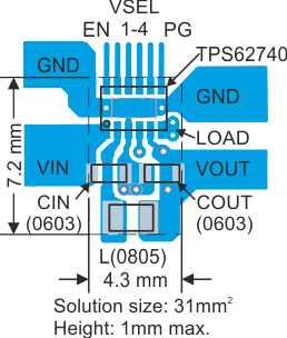 Figure 43. Recommended PCB Layout