SLVSB02B November 2013 – July 2014 TPS62740 , TPS62742
PRODUCTION DATA.
- 1 Features
- 2 Applications
- 3 Description
- 4 Revision History
- 5 Device Comparison Table
- 6 Specifications
- 7 Detailed Description
- 8 Application and Implementation
- 9 Power Supply Recommendations
- 10Layout
- 11Device and Documentation Support
- 12Mechanical, Packaging, and Orderable Information
Package Options
Mechanical Data (Package|Pins)
- DSS|12
Thermal pad, mechanical data (Package|Pins)
- DSS|12
Orderable Information
Pin Configuration and Functions
WSON PACKAGE
12-Pin
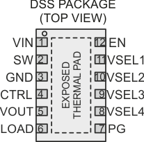
Pin Functions
| PIN | I/O | DESCRIPTION | |
|---|---|---|---|
| NAME | NO | ||
| VIN | 1 | PWR | VIN power supply pin. Connect this pin close to the VIN terminal of the input capacitor. A ceramic capacitor of 4.7µF is required. |
| SW | 2 | OUT | This is the switch pin and is connected to the internal MOSFET switches. Connect the inductor to this terminal. |
| GND | 3 | PWR | GND supply pin. Connect this pin close to the GND terminal of the input and output capacitor. |
| CTRL | 4 | IN | This pin controls the output LOAD pin. With CTRL = low, the output LOAD is disabled. This pin must be terminated. |
| VOUT | 5 | IN | Feedback pin for the internal feedback divider network and regulation loop. An internal load switch is connected between this pin and the LOAD pin. Connect this pin directly to the output capacitor with a short trace. |
| LOAD | 6 | OUT | This output is controlled by the CTRL Pin. With CTRL high, an internal load switch connects the LOAD pin to the VOUT pin. The LOAD pin allows to connect / disconnect other system components to the output of the DC/DC converter. This pin is pulled to GND with CTRL pin = low. The LOAD pin features a soft switching. If not used, leave the pin open. |
| PG | 7 | OUT | Power good open drain output. This pin is high impedance to indicate "Power Good". Connect a external pull up resistor to generate a "high" level. If not used, this pin can be left open. |
| VSEL4 | 8 | IN | Output voltage selection pins. See Table 1 for VOUT selection. These pins must be terminated and can be changed during operation. |
| VSEL3 | 9 | IN | |
| VSEL2 | 10 | IN | |
| VSEL1 | 11 | IN | |
| EN | 12 | IN | High level enables the devices, low level turns the device into shutdown mode. This pin must be terminated. |
| EXPOSED THERMAL PAD | NC | Not electrically connected to the IC, but must be soldered. Connect this pad to GND and use it as a central GND plane. | |
Table 1. Output Voltage Setting
| Device | VOUT | VSEL 4 | VSEL 3 | VSEL 2 | VSEL 1 |
|---|---|---|---|---|---|
| TPS62740 / 42 | 1.8 | 0 | 0 | 0 | 0 |
| 1.9 | 0 | 0 | 0 | 1 | |
| 2.0 | 0 | 0 | 1 | 0 | |
| 2.1 | 0 | 0 | 1 | 1 | |
| 2.2 | 0 | 1 | 0 | 0 | |
| 2.3 | 0 | 1 | 0 | 1 | |
| 2.4 | 0 | 1 | 1 | 0 | |
| 2.5 | 0 | 1 | 1 | 1 | |
| 2.6 | 1 | 0 | 0 | 0 | |
| 2.7 | 1 | 0 | 0 | 1 | |
| 2.8 | 1 | 0 | 1 | 0 | |
| 2.9 | 1 | 0 | 1 | 1 | |
| 3.0 | 1 | 1 | 0 | 0 | |
| 3.1 | 1 | 1 | 0 | 1 | |
| 3.2 | 1 | 1 | 1 | 0 | |
| 3.3 | 1 | 1 | 1 | 1 |