SLVSCX0B February   2016  – April 2016 TPS62770

PRODUCTION DATA.  

  1. Features
  2. Applications
  3. Description
  4. Revision History
  5. Pin Configuration and Functions
    1. 5.1 Output Voltage Setting Step-Down Converter
  6. Specifications
    1. 6.1 ESD Ratings
    2. 6.2 Thermal Information
    3. 6.3 Electrical Characteristics
    4. 6.4 Typical Characteristics
  7. Detailed Description
    1. 7.1 Overview
    2. 7.2 Functional Block Diagram
    3. 7.3 Feature Description
      1. 7.3.1 Step-Down Converter Device
        1. 7.3.1.1 DCS-Control
        2. 7.3.1.2 Output Voltage Selection with pins VSEL1-VSEL3
        3. 7.3.1.3 CTRL / Output Load
        4. 7.3.1.4 Output Discharge At Pins VO1 And LOAD
        5. 7.3.1.5 Undervoltage Lockout UVLO
        6. 7.3.1.6 Short Circuit Protection
      2. 7.3.2 Step-Up Converter Device
        1. 7.3.2.1 Under-Voltage Lockout
        2. 7.3.2.2 Output Disconnect
        3. 7.3.2.3 12 V Fixed Output Voltage
        4. 7.3.2.4 Mode Selection With Pin BM
        5. 7.3.2.5 Output Overvoltage Protection
        6. 7.3.2.6 Output Short Circuit Protection
        7. 7.3.2.7 PWM to Analog Converter AT PIN EN2/PWM
    4. 7.4 Device Functional Modes
      1. 7.4.1 Step-Down Converter
        1. 7.4.1.1 Enable and Shutdown
        2. 7.4.1.2 Power Save Mode Operation
        3. 7.4.1.3 PWM Mode Operation
        4. 7.4.1.4 Device Start-up and Soft Start
        5. 7.4.1.5 Automatic Transition Into 100% Mode
      2. 7.4.2 Step-Up Converter
        1. 7.4.2.1 Enable and Shutdown
        2. 7.4.2.2 Soft Start
        3. 7.4.2.3 Power Save Mode
        4. 7.4.2.4 PWM Mode
        5. 7.4.2.5 Constant-Current Step-Up Mode Operation
        6. 7.4.2.6 Constant-Voltage Step-Up Mode Operation
  8. Application and Implementation
    1. 8.1 Application Information
    2. 8.2 Typical Applications
      1. 8.2.1 TPS62770 Step-Down Converter + Load Switch
        1. 8.2.1.1 Design Requirements
        2. 8.2.1.2 Detailed Design Procedure
          1. 8.2.1.2.1 Setting The Output Voltage Of The Step-Down Converter
          2. 8.2.1.2.2 Inductor Selection Step-Down Converter
          3. 8.2.1.2.3 Input and Output Capacitor Selection
        3. 8.2.1.3 Application Curves - TPS62770 Step-Down Converter + Load Switch
      2. 8.2.2 TPS62770 Step-Up Converter with Adjustable Output Voltage (9 V to 15 V)
        1. 8.2.2.1 Design Requirements
        2. 8.2.2.2 Detailed Design Procedure
          1. 8.2.2.2.1 Programming the Output Voltage Of The Step-Up Converter
          2. 8.2.2.2.2 Inductor Selection for TPS62770 Step-Up Converter
            1. 8.2.2.2.2.1 Example Step-Up Converter with 12-V Fixed Output
        3. 8.2.2.3 Application Curves for Step-Up Converter
      3. 8.2.3 Step-Up Converter with Constant 5-V Output Voltage
        1. 8.2.3.1 Design Requirements
        2. 8.2.3.2 Detailed Design Procedure
        3. 8.2.3.3 Application Performance Curves
      4. 8.2.4 Typical Step Up Converter with Constant Output Current
        1. 8.2.4.1 Design Requirements
        2. 8.2.4.2 Detailed Design Procedure
          1. 8.2.4.2.1 Setting the Output Current
          2. 8.2.4.2.2 Inductor Selection
        3. 8.2.4.3 Application Curves
  9. Power Supply Recommendations
  10. 10Layout
    1. 10.1 Layout Guidelines
    2. 10.2 Layout Example
  11. 11Device and Documentation Support
    1. 11.1 Device Support
      1. 11.1.1 Third-Party Products Disclaimer
    2. 11.2 Documentation Support
      1. 11.2.1 Related Documentation
    3. 11.3 Trademarks
    4. 11.4 Electrostatic Discharge Caution
    5. 11.5 Glossary
  12. 12Mechanical, Packaging, and Orderable Information

Package Options

Mechanical Data (Package|Pins)
Thermal pad, mechanical data (Package|Pins)
Orderable Information

10 Layout

10.1 Layout Guidelines

  • As for all switching power supplies, the layout is an important step in the design. Care must be taken in board layout to get the specified performance.
  • If the layout is not carefully done, the regulator could show poor line and/or load regulation, stability issues as well as EMI problems and interference with RF circuits.
  • It is critical to provide a low inductance, impedance ground path. Therefore, use wide and short traces for the main current paths.
  • The input capacitor should be placed as close as possible to the IC pins VIN and GND. The output capacitors should be placed close between VO1/2 and GND pins.
  • The VO1/2 line should be connected to the output capacitor and routed away from noisy components and traces (e.g. SW line) or other noise sources.
  • See Figure 45 and Figure 46 for the recommended PCB layout.

10.2 Layout Example
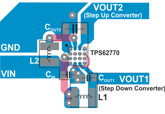
TPS62770 TPS62770_SolSize.gif Figure 45. Recommended PCB Layout with 12 V Fixed VOUT2
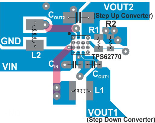
TPS62770 TPS62770_Flexible.gif Figure 46. Recommended PCB Layout with Adjustable VOUT2