SLVSEF9I March   2018  – March 2024 TPS62824 , TPS62824A , TPS62825 , TPS62825A , TPS62826 , TPS62826A , TPS62827 , TPS62827A

PRODUCTION DATA  

  1.   1
  2. Features
  3. Applications
  4. Description
  5. Device Options
  6. Pin Configuration and Functions
  7. Specifications
    1. 6.1 Absolute Maximum Ratings
    2. 6.2 ESD Ratings
    3. 6.3 Recommended Operating Conditions
    4. 6.4 Thermal Information
    5. 6.5 Electrical Characteristics
    6. 6.6 Typical Characteristics
  8. Detailed Description
    1. 7.1 Overview
    2. 7.2 Functional Block Diagram
    3. 7.3 Feature Description
      1. 7.3.1 Pulse Width Modulation (PWM) Operation
      2. 7.3.2 Power Save Mode (PSM) Operation
      3. 7.3.3 Minimum Duty Cycle and 100% Mode Operation
      4. 7.3.4 Soft Start
      5. 7.3.5 Switch Current Limit and HICCUP Short-Circuit Protection
      6. 7.3.6 Undervoltage Lockout
      7. 7.3.7 Thermal Shutdown
    4. 7.4 Device Functional Modes
      1. 7.4.1 Enable, Disable, and Output Discharge
      2. 7.4.2 Power Good
  9. Application and Implementation
    1. 8.1 Application Information
    2. 8.2 Typical Application
      1. 8.2.1 Design Requirements
      2. 8.2.2 Detailed Design Procedure
        1. 8.2.2.1 Custom Design With WEBENCH® Tools
        2. 8.2.2.2 Setting The Output Voltage
        3. 8.2.2.3 Output Filter Design
        4. 8.2.2.4 Inductor Selection
        5. 8.2.2.5 Capacitor Selection
      3. 8.2.3 Application Curves
    3. 8.3 Power Supply Recommendations
    4. 8.4 Layout
      1. 8.4.1 Layout Guidelines
      2. 8.4.2 Layout Example
        1. 8.4.2.1 Thermal Considerations
  10. Device and Documentation Support
    1. 9.1 Device Support
      1. 9.1.1 Third-Party Products Disclaimer
      2. 9.1.2 Development Support
        1. 9.1.2.1 Custom Design With WEBENCH® Tools
    2. 9.2 Documentation Support
      1. 9.2.1 Related Documentation
    3. 9.3 Support Resources
    4. 9.4 Trademarks
    5. 9.5 Electrostatic Discharge Caution
    6. 9.6 Glossary
  11. 10Revision History
  12. 11Mechanical, Packaging, and Orderable Information

Package Options

Mechanical Data (Package|Pins)
Thermal pad, mechanical data (Package|Pins)
Orderable Information

Application Curves

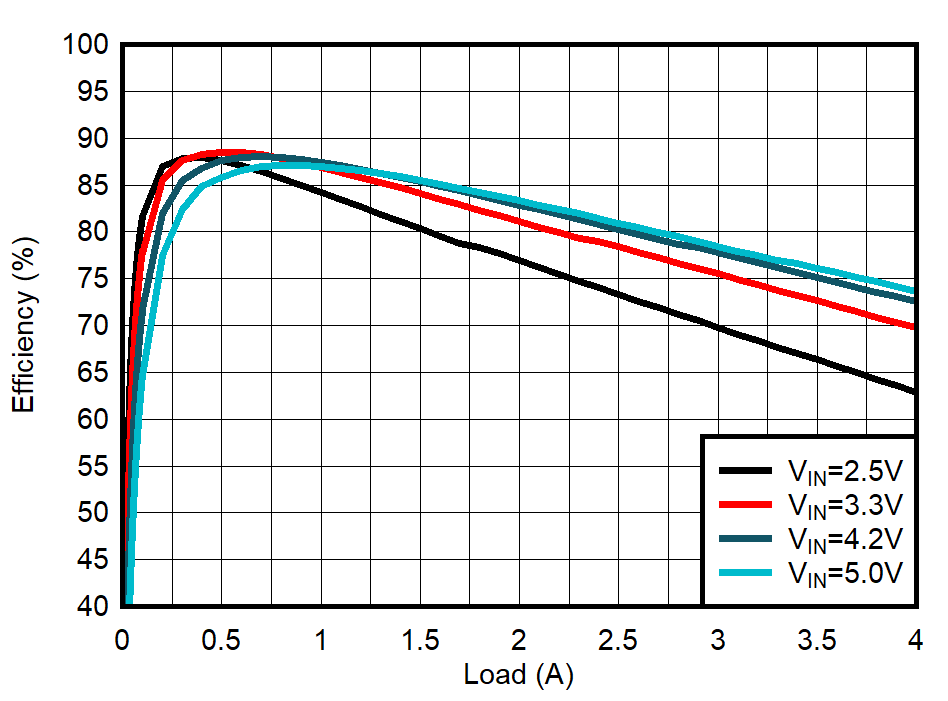
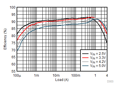
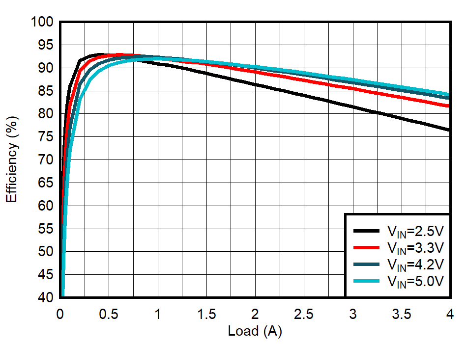
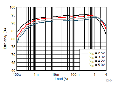
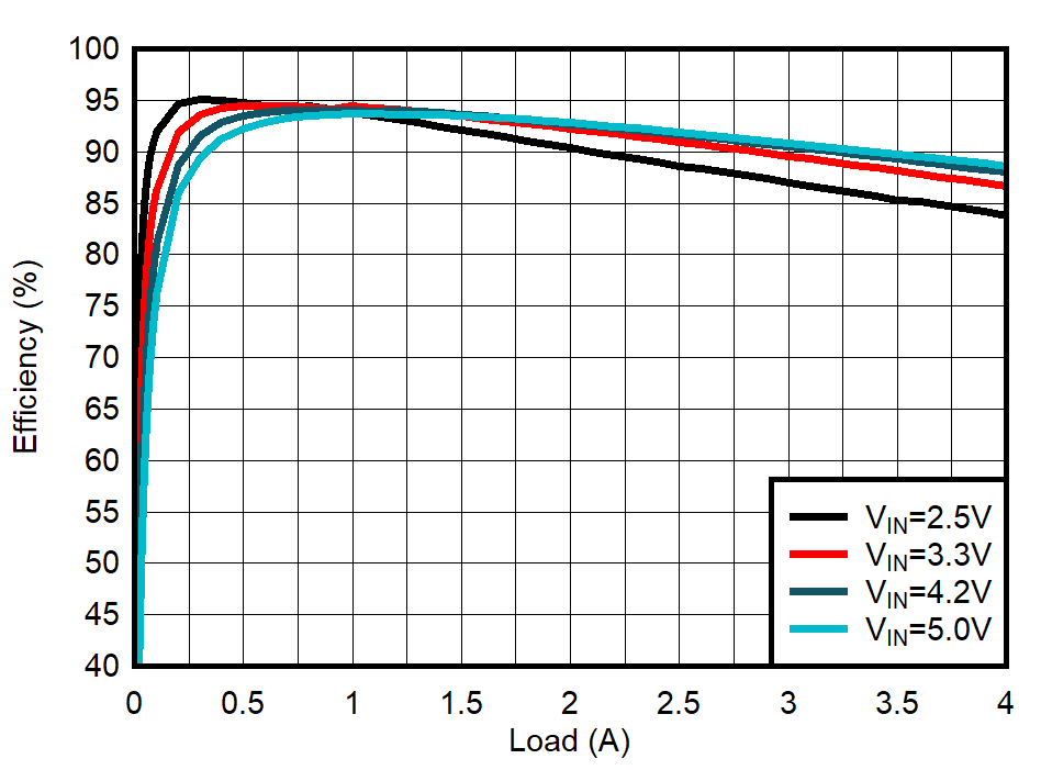
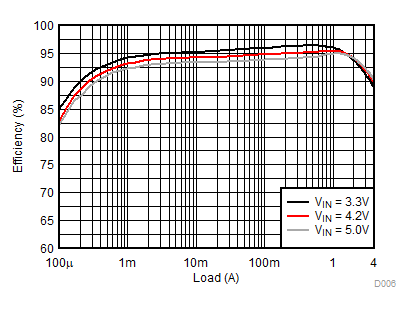
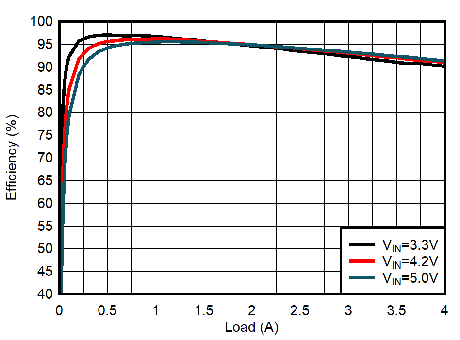
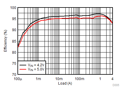
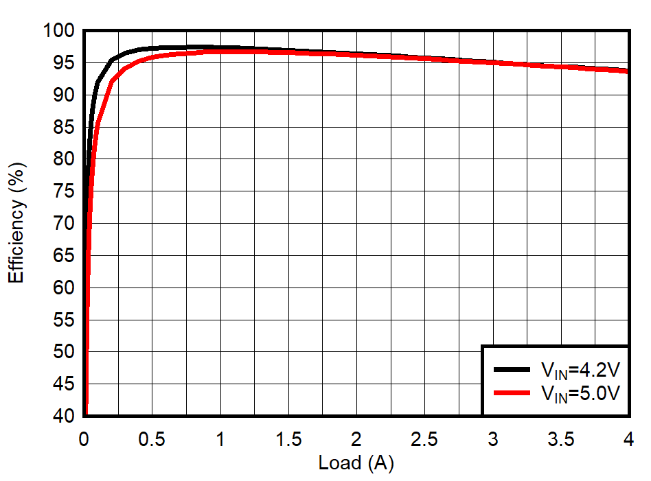
VIN = 5.0V, VOUT = 1.8V, TA = 25°C, BOM = Table 8-2, unless otherwise noted.
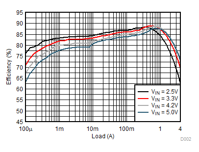
GUID-A5262459-C723-4203-B817-6F4E27B170AD-low.gif
VOUT = 0.6V
Figure 8-3 Efficiency
GUID-20201005-CA0I-FRWC-MXQ1-5ND0HWL8M2FB-low.gif
VOUT = 0.6V F-PWM devices
Figure 8-5 PWM Efficiency
GUID-2962B9B3-F8A6-465C-984A-6DEA85D7108A-low.gif
VOUT = 1.2V
Figure 8-7 Efficiency
GUID-20201005-CA0I-54V0-DTLF-FR9FXFZXSWTQ-low.gif
VOUT = 1.2V F-PWM devices
Figure 8-9 PWM Efficiency
GUID-18382729-9F82-48C8-833E-45EB64D324FD-low.gif
VOUT = 1.8V
Figure 8-11 Efficiency
GUID-20201005-CA0I-CV7N-XMF9-987C8961TTDZ-low.gif
VOUT = 1.8V F-PWM devices
Figure 8-13 PWM Efficiency
GUID-3E505F03-0508-4E8C-ADDF-FD49B57B37E5-low.gif
VOUT = 2.5V
Figure 8-15 Efficiency
GUID-20201005-CA0I-2PXT-QCRT-43ZW063GS4KZ-low.gif
VOUT = 2.5V F-PWM devices
Figure 8-17 PWM Efficiency
GUID-A9AAD678-6EB3-4ABA-B3C7-9D4FC3E54317-low.gif
VOUT = 3.3V
Figure 8-19 Efficiency
GUID-20201005-CA0I-2KZJ-HKRN-8Q0X7BX81X1X-low.gif
VOUT = 3.3V F-PWM devices
Figure 8-21 PWM Efficiency
GUID-F6901B74-FAF6-4DC1-898C-1D82FE057615-low.gif
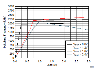
VIN = 3.3V TPS62824, TPS62825, TPS62826
Figure 8-23 Switching Frequency
GUID-20201112-CA0I-ZQ3S-5FR6-VF9GKLMXLVZC-low.gif
VIN = 3.3V TPS62824A/5A/6A/7A
Figure 8-25 Switching Frequency
GUID-E3AB4F4A-2F93-4B7F-9B13-987F4D54809C-low.gif
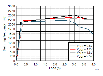
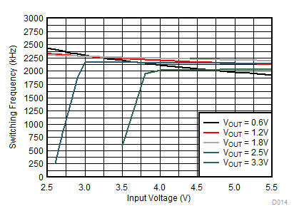
VIN = 3.3V TPS62827
Figure 8-27 Switching Frequency
GUID-218E8B07-072C-437F-B00C-71F8C9AB6757-low.gif
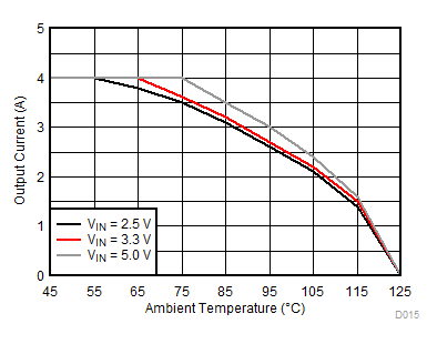
VOUT = 1.2V θJA= 71.4°C/W
Figure 8-29 Thermal Derating
GUID-EF95438C-CB89-4F5E-AA48-965F1763BAF1-low.gif
VOUT = 2.5V θJA= 71.4°C/W
Figure 8-31 Thermal Derating
GUID-288F28E3-BED6-474A-9D1E-C96193C48C38-low.gif
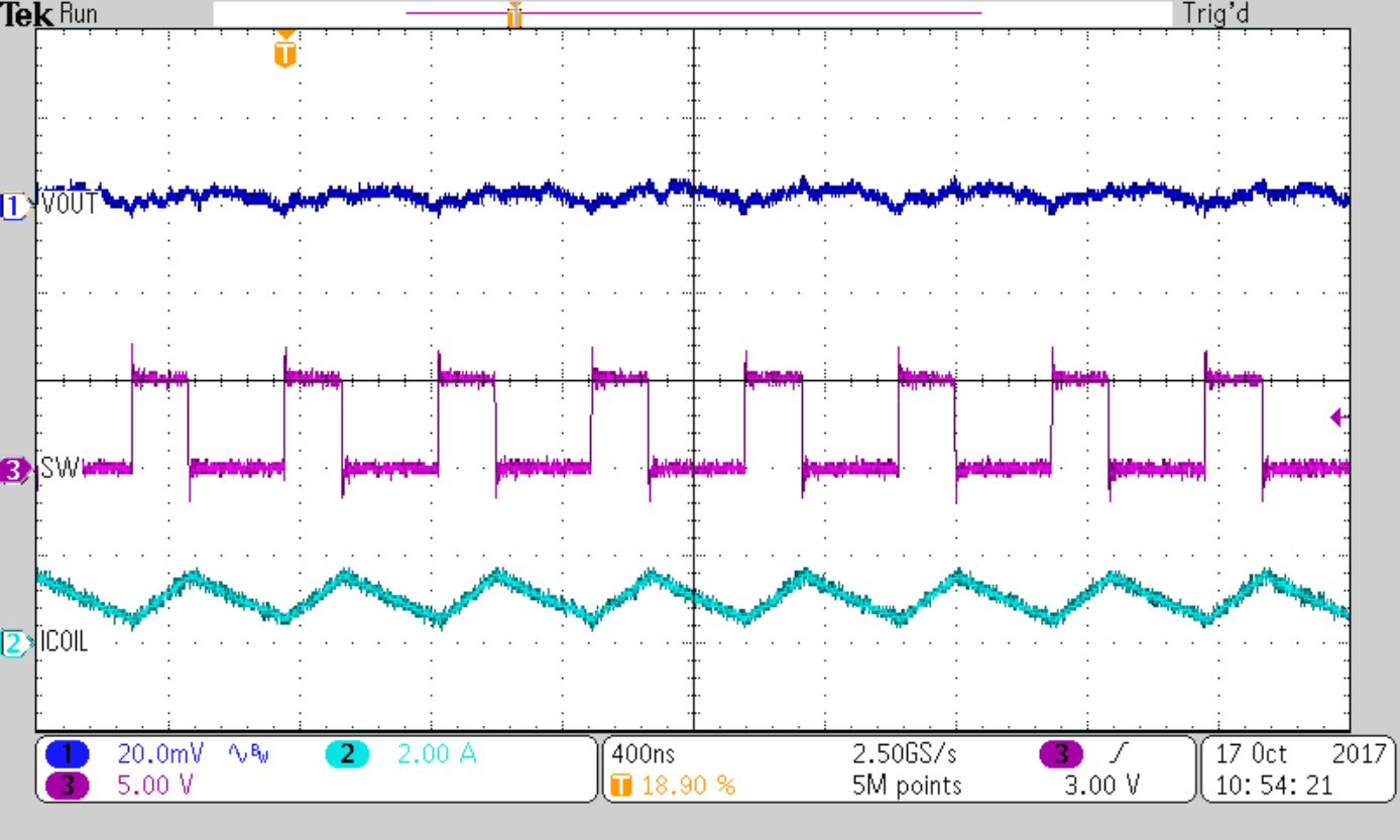
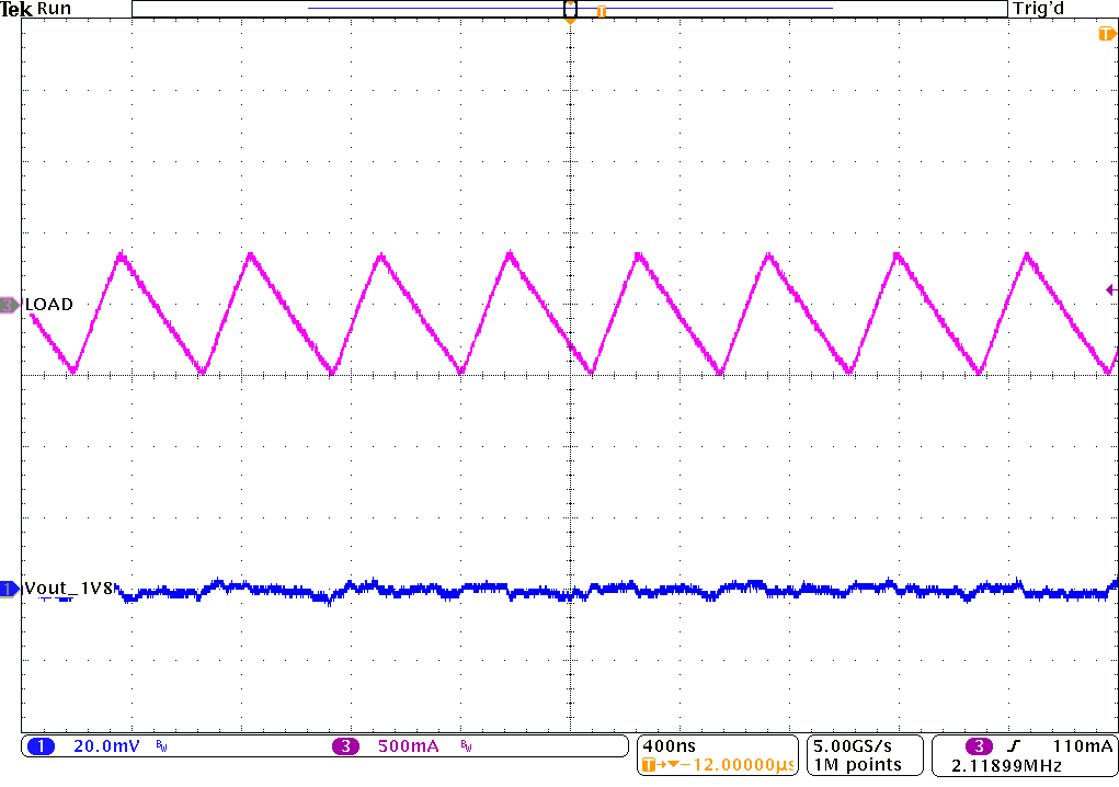
IOUT = 1.0A TPS62824/5/6/7
Figure 8-33 PWM Operation
GUID-20201008-CA0I-VQ9C-BJCB-X7GRSS0GSMT4-low.png
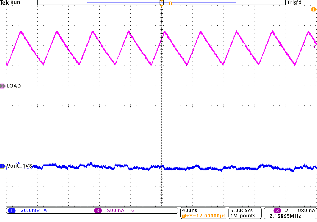
IOUT = 1.0A TPS62824A/5A/6A/7A
Figure 8-35 PWM Operation at F-PWM
GUID-F58770CB-E531-4D0E-960F-7FA8633ED7F3-low.gif
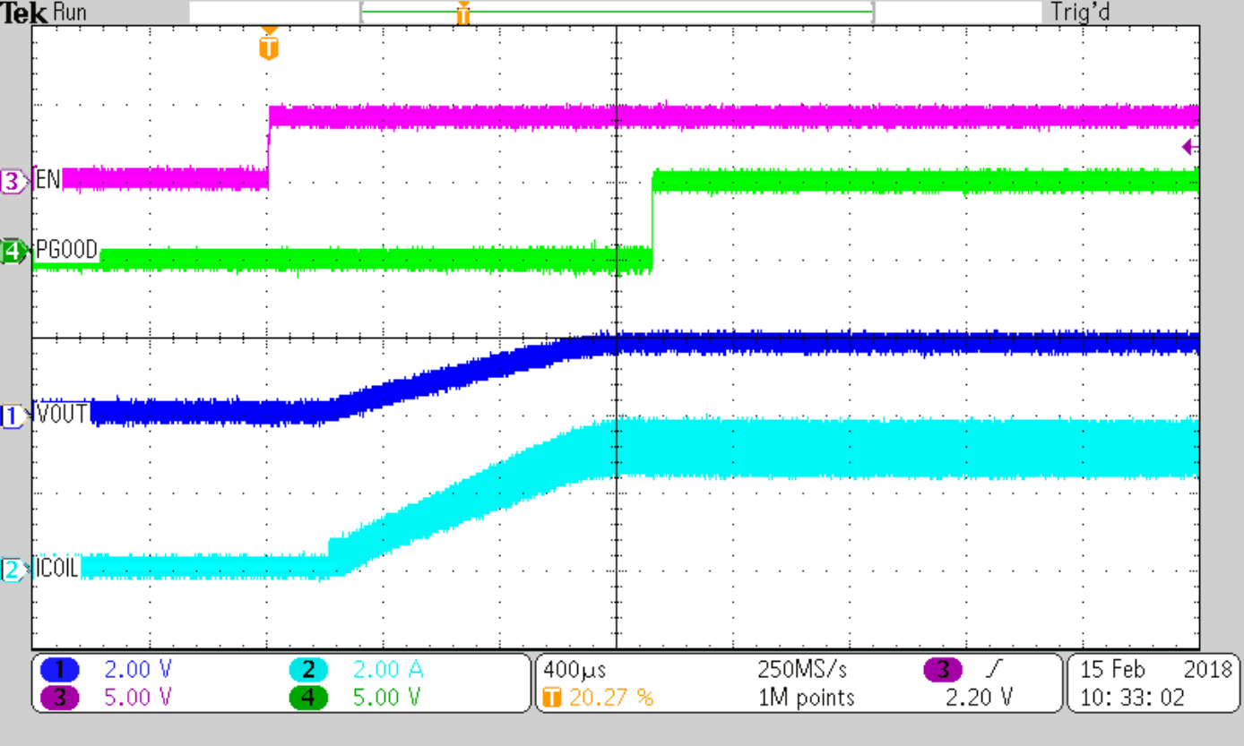
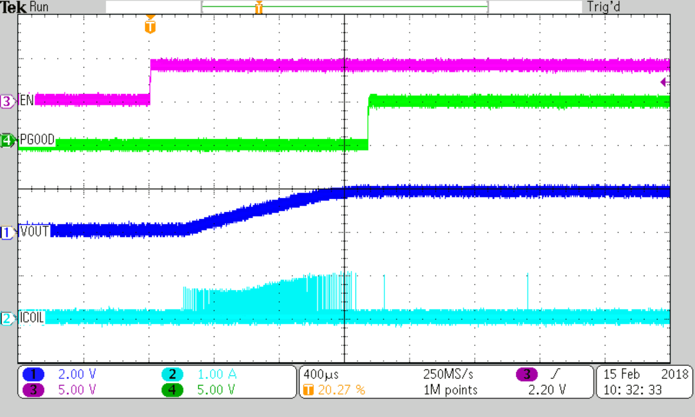
Load = 0.6Ω TPS62826
Figure 8-37 Start-Up With Load
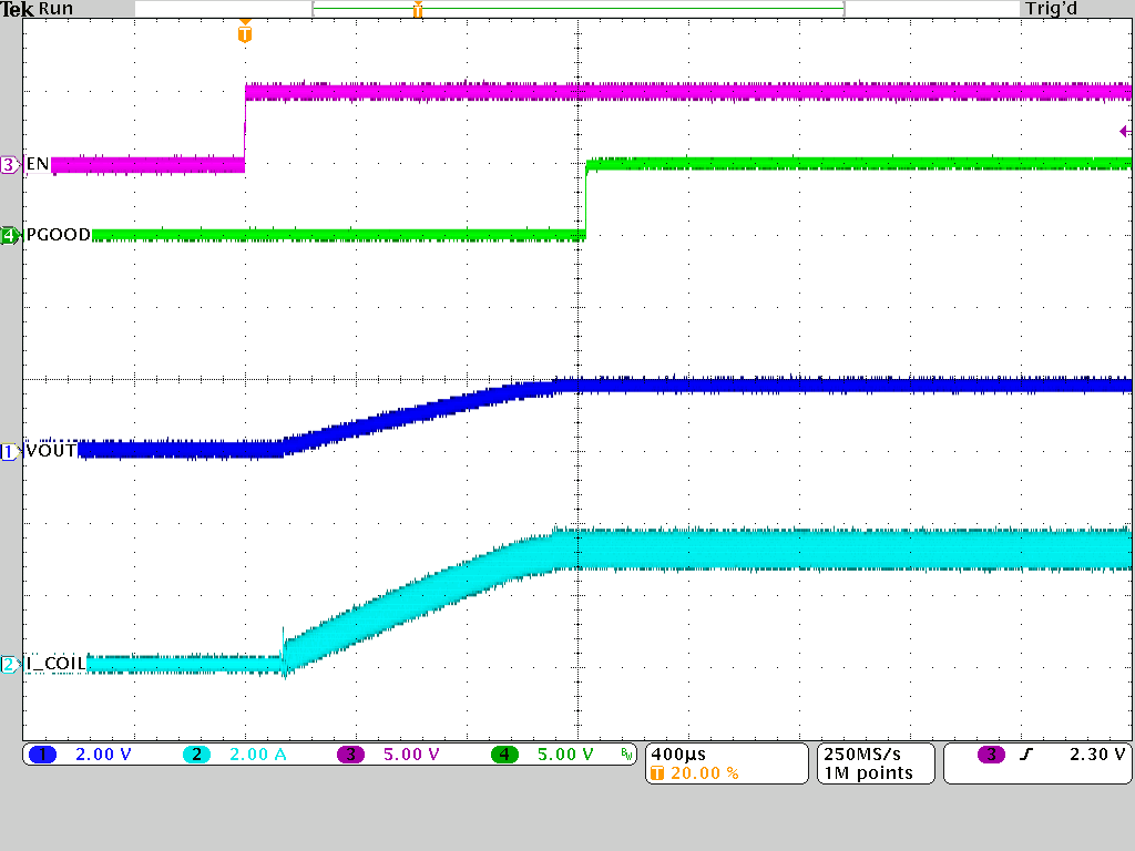
GUID-20201007-CA0I-1GJS-CVLZ-VS2QWT86SSHT-low.png
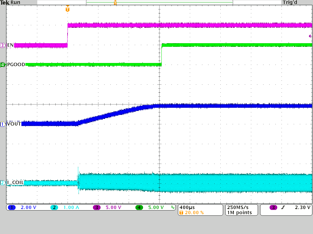
Load = 0.6Ω TPS62826A/7A
Figure 8-39 Start-Up With Load
GUID-55CF06F1-B6AF-4B62-9201-1641095605DC-low.gif
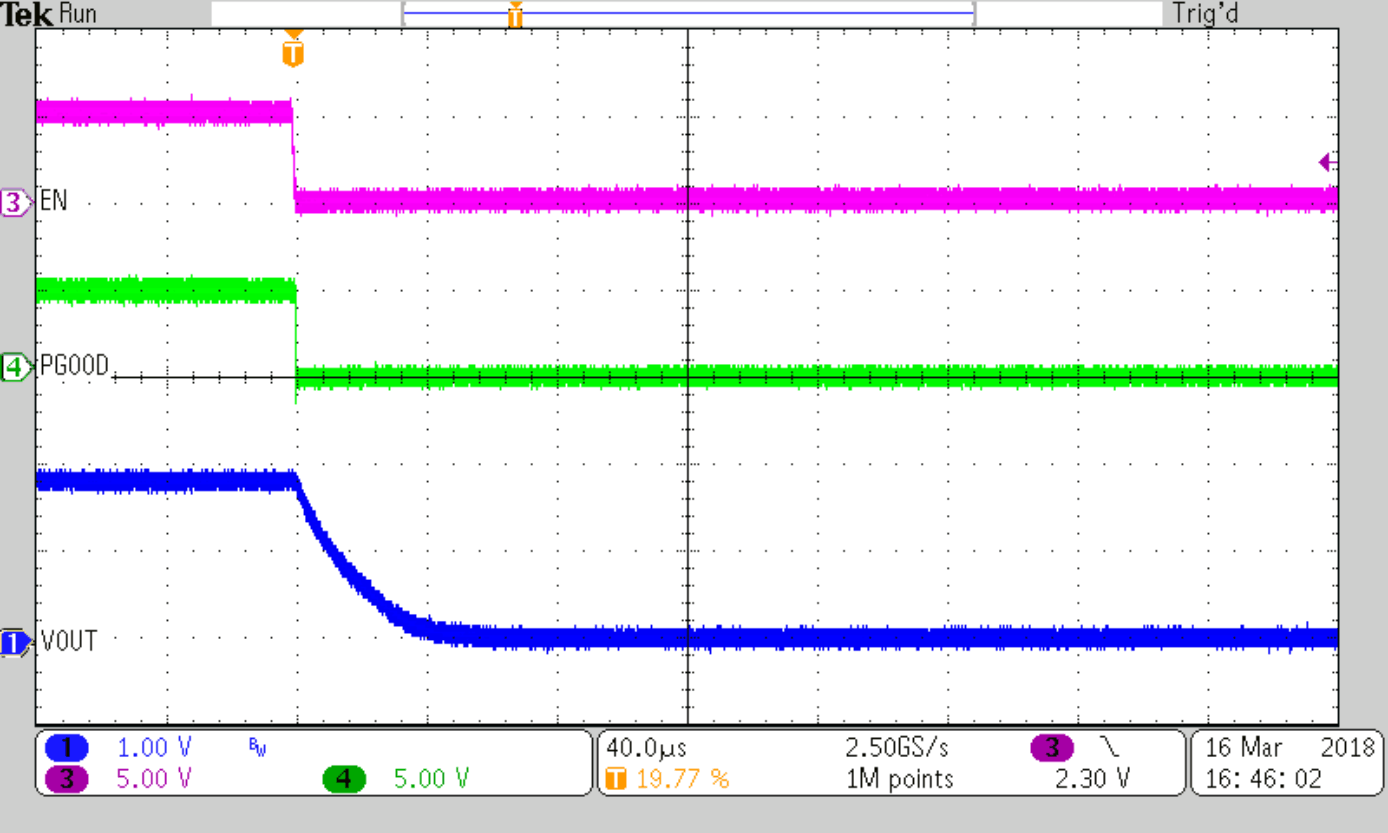
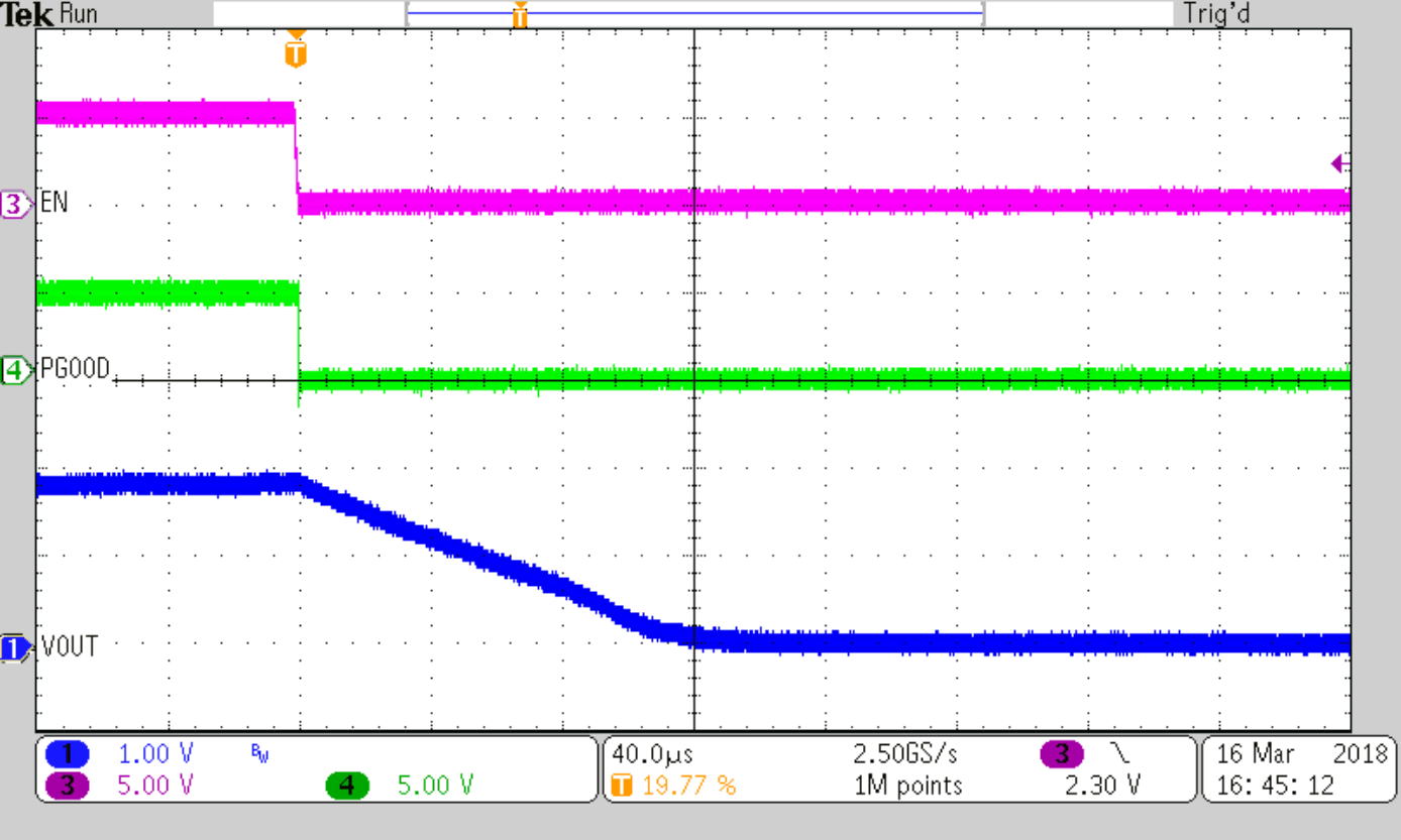
Load = 1.8Ω TPS6282x
Figure 8-41 Disable, Active Output Discharge
GUID-374A6018-D78C-4829-B853-26078AA0FE2F-low.gif
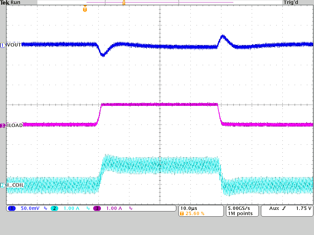
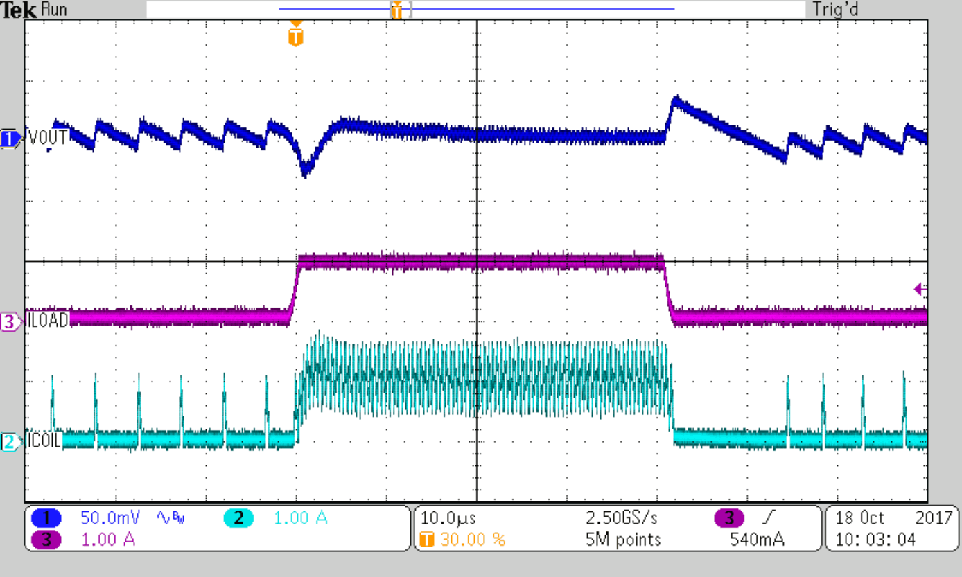
IOUT = 0.05A to 1A TPS62824/5/6/7
Figure 8-43 Load Transient
GUID-20201007-CA0I-T1GP-ZZ1Q-ZFDNTFF8JM35-low.png
IOUT = 0.05A to 1A TPS62824A/5A/6A/7A
Figure 8-45 Load Transient
GUID-9A85FC9C-7064-426B-BA0D-255665EC0017-low.gif
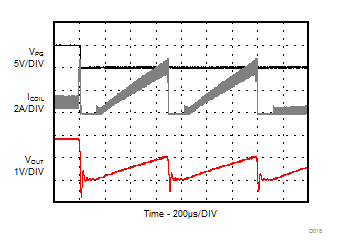
IOUT = 1A TPS6282x
Figure 8-47 HICCUP Short-Circuit Protection
GUID-F9E688C6-7366-4F62-9479-AF610EAD32A6-low.gif
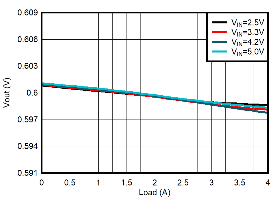
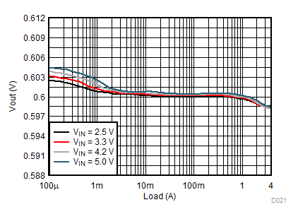
VOUT = 0.6V
Figure 8-4 Load Regulation
GUID-20201005-CA0I-9J0N-NP1W-R0ZZKZ1HJ2BM-low.gif
VOUT = 0.6V F-PWM devices
Figure 8-6 Load Regulation
GUID-1081B9F6-7B3C-4A2E-9930-150245DFD886-low.gif
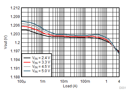
VOUT = 1.2V
Figure 8-8 Load Regulation
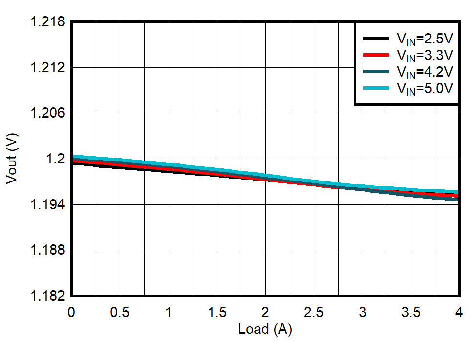
GUID-20201005-CA0I-HHRW-L0ZL-Z5CWKFL71WX5-low.gif
VOUT = 1.2V F-PWM devices
Figure 8-10 Load Regulation
GUID-CAE4190D-50A6-4AEB-AB26-5C352F754A02-low.gif
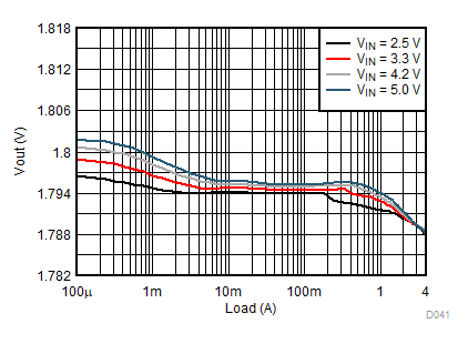
VOUT = 1.8V
Figure 8-12 Load Regulation
GUID-20201005-CA0I-M6NL-7HX1-VKVKL29M0QWD-low.gif
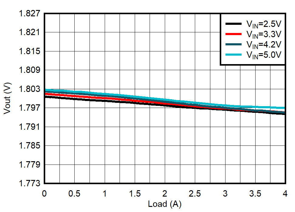
VOUT = 1.8V F-PWM devices
Figure 8-14 Load Regulation
GUID-B382DB33-F475-4812-9C86-C4C04FF97C0B-low.gif
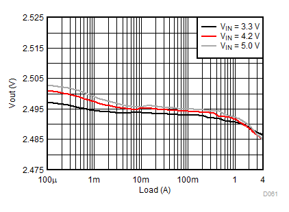
VOUT = 2.5V
Figure 8-16 Load Regulation
GUID-20201005-CA0I-2MRT-WTLW-RKSZWCRCKHZW-low.gif
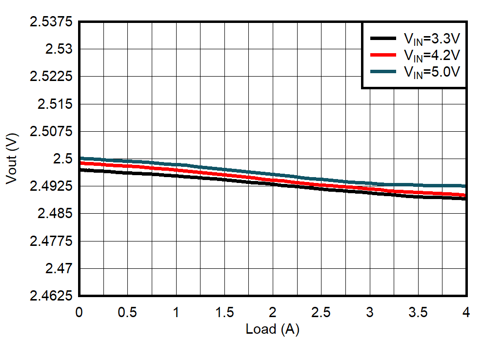
VOUT = 2.5V F-PWM devices
Figure 8-18 Load Regulation
GUID-C0B7C5A8-CB1A-47DB-8FA4-B053145F8B31-low.gif
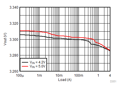
VOUT = 3.3V
Figure 8-20 Load Regulation
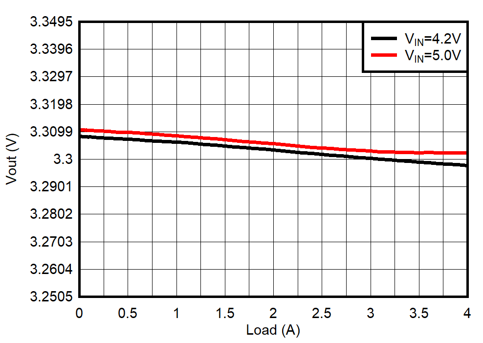
GUID-20201005-CA0I-W8G0-KRCG-TJTRXDQR8ZJQ-low.gif
VOUT = 3.3V F-PWM devices
Figure 8-22 Load Regulation
GUID-094FFC6D-05D7-45AD-9628-643F4C423281-low.gif
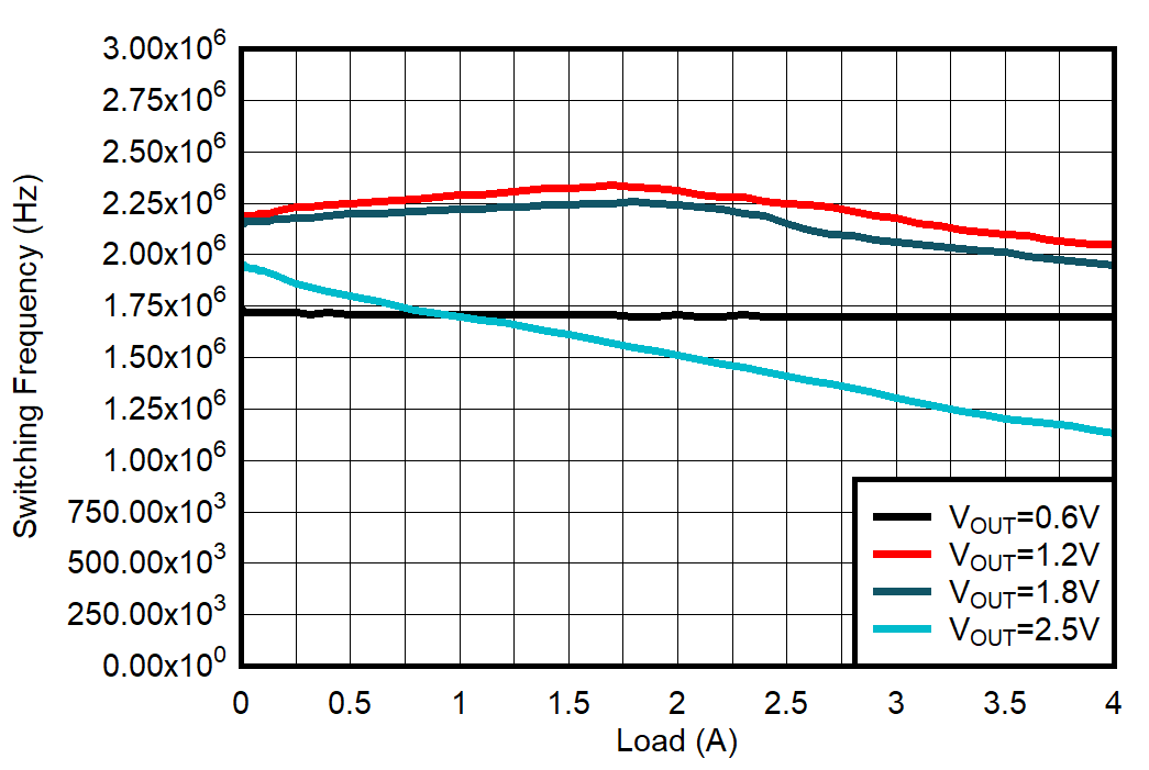
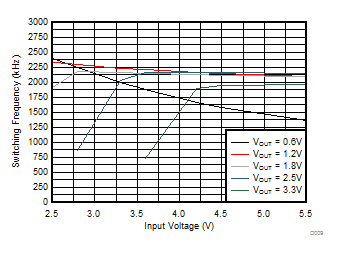
IOUT = 1.0A TPS62824, TPS62825, TPS62826
Figure 8-24 Switching Frequency
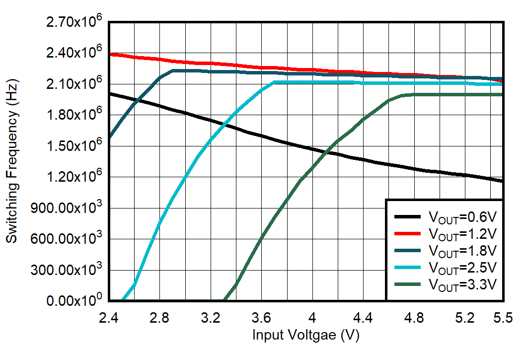
GUID-20201112-CA0I-KX7T-RJFG-63DTVWRDRCKH-low.gif
IOUT = 1.0A TPS62824A/5A/6A/7A
Figure 8-26 Switching Frequency
GUID-2B344D5D-768E-4483-A67E-39D799356A05-low.gif
IOUT = 1.0A TPS62827
Figure 8-28 Switching Frequency
GUID-E2D213A4-FA01-45FC-8BC0-F7FBE62E44CE-low.gif
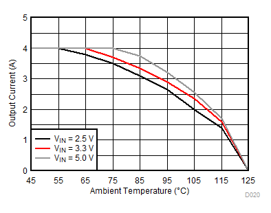
VOUT = 1.8V θJA= 71.4°C/W
Figure 8-30 Thermal Derating
GUID-DDD300C1-5227-48A0-B12E-2571ABBE0604-low.gif
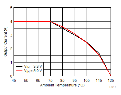
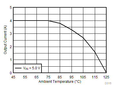
VOUT = 3.3V θJA= 71.4°C/W
Figure 8-32 Thermal Derating
GUID-7711387C-8BA9-452A-A71A-0B93D51D6709-low.gif
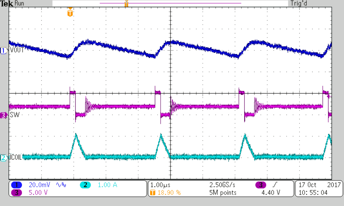
IOUT = 0.1A TPS62824/5/6/7
Figure 8-34 PSM Operation
GUID-20201008-CA0I-KSCW-C1TG-PS5QHRVXD06C-low.png
No load TPS62824A/5A/6A/7A
Figure 8-36 PWM Operation at F-PWM
GUID-18D5903F-80E4-496E-9375-91B5D227A719-low.gif
TPS62824/5/6
Figure 8-38 Start-Up With No Load
GUID-20201007-CA0I-KCFN-X60T-TVSD7RS3NWLT-low.png
TPS62824A/5A/6A/7A
Figure 8-40 Start-Up With No Load
GUID-0254B80A-EBF9-4292-9929-70A9624F818D-low.gif
TPS6282x
Figure 8-42 Disable, Active Output Discharge at No Load
GUID-EA490D81-C621-472D-8468-321EB95EF1E4-low.gif
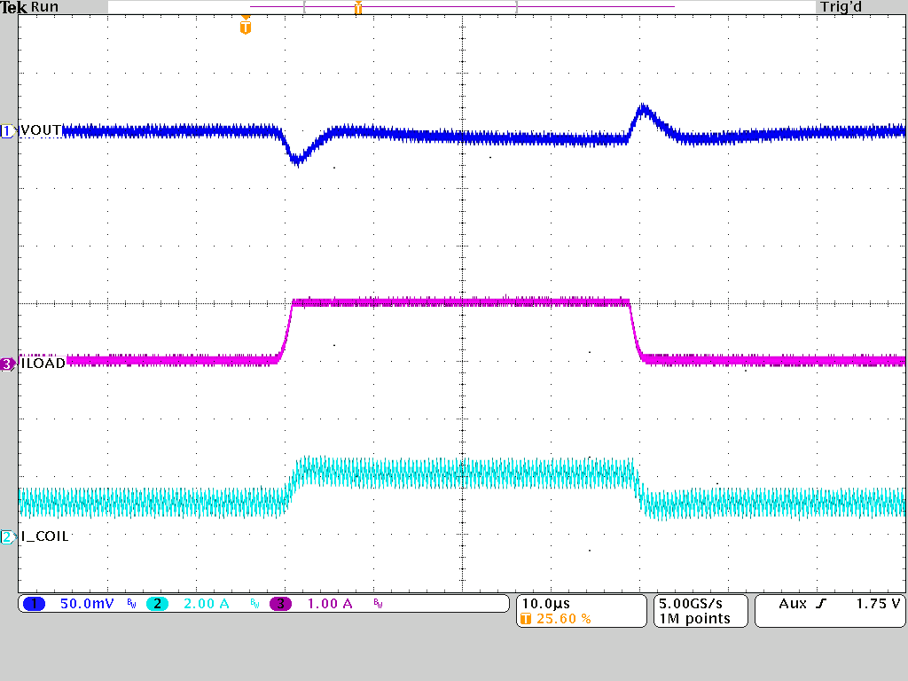
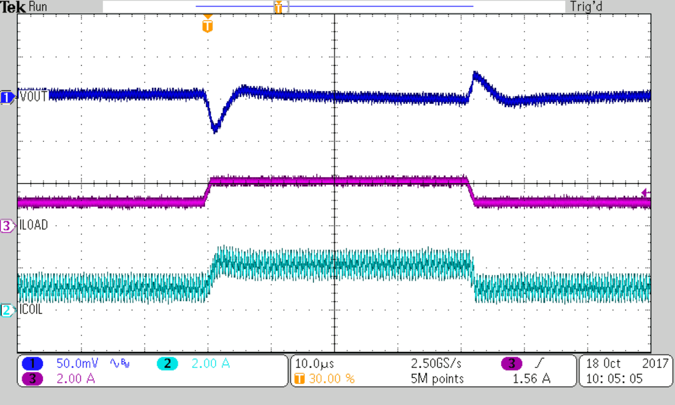
IOUT = 1A to 2A TPS62825/6/7
Figure 8-44 Load Transient
GUID-20201007-CA0I-HNJX-K4WG-WHVVDJNJFKHB-low.png
IOUT = 1A to 2A TPS62825A/6A/7A
Figure 8-46 Load Transient
GUID-FB50DDDB-E920-46B9-9B27-7CEF6A9A5D72-low.gif
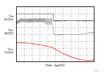
IOUT = 1A TPS6282x
Figure 8-48 HICCUP Short-Circuit Protection (Zoom In)