SLVSEC6D June 2019 – March 2020 TPS62840
PRODUCTION DATA.
- 1 Features
- 2 Applications
- 3 Description
- 4 Revision History
- 5 Device Comparison Table
- 6 Pin Configuration and Functions
- 7 Specifications
-
8 Detailed Description
- 8.1 Overview
- 8.2 Functional Block Diagram
- 8.3
Feature Description
- 8.3.1 Smart Enable and Shutdown
- 8.3.2 Soft Start
- 8.3.3 Mode Selection: Power-Save Mode (PFM/PWM) or Forced PWM Operation (FPWM)
- 8.3.4 Output Voltage Selection (VSET)
- 8.3.5 Undervoltage Lockout UVLO
- 8.3.6 Switch Current Limit / Short Circuit Protection
- 8.3.7 Output Voltage Discharge
- 8.3.8 Thermal Shutdown
- 8.3.9 STOP Mode
- 8.4 Device Functional Modes
- 9 Application and Implementation
- 10Power Supply Recommendations
- 11Layout
- 12Device and Documentation Support
- 13Mechanical, Packaging, and Orderable Information
Package Options
Mechanical Data (Package|Pins)
Thermal pad, mechanical data (Package|Pins)
- DLC|8
Orderable Information
7.6 Typical Characteristics
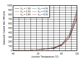
| EN = VIN | VOUT = 1.55 V | Device Not Switching |
(IQ_VIN)
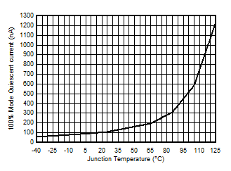
| EN = VIN | VIN = VOUT = 3.3 V | Device Not Switching |
(IQ_100%_MODE)
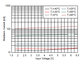
| EN = GND |
(ISD)
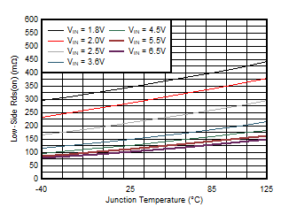 Figure 7. Low-Side RDSON versus Temperature
(DLC, YBG packages)
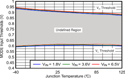 Figure 9. MODE Input Thresholds versus Temperature
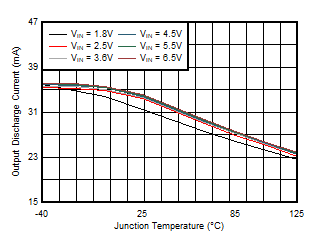
| EN = GND | VOUT = 1.8 V |
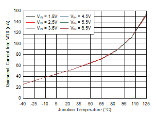
| EN = VIN | VOUT = 1.55 V | Device Not Switching |
(IQ_VOS)
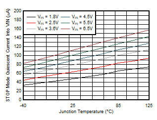
| EN = VIN | VOUT = 1.8 V | Device Not Switching |
(IQ_VIN_STOP)
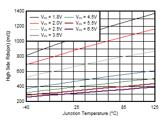
(DLC, YBG packages)
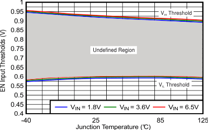 Figure 8. EN Input Thresholds versus Temperature
 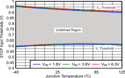 Figure 10. STOP Input Thresholds versus Temperature