SLUSDM0J May   2020  – November 2023 TPS628501-Q1 , TPS628502-Q1 , TPS628503-Q1

PRODUCTION DATA  

  1.   1
  2. Features
  3. Applications
  4. Description
  5. Device Comparison Table
  6. Pin Configuration and Functions
  7. Specifications
    1. 6.1 Absolute Maximum Ratings
    2. 6.2 ESD Ratings
    3. 6.3 Recommended Operating Conditions
    4. 6.4 Thermal Information
    5. 6.5 Electrical Characteristics
    6. 6.6 Typical Characteristics
  8. Parameter Measurement Information
    1. 7.1 Schematic
  9. Detailed Description
    1. 8.1 Overview
    2. 8.2 Functional Block Diagram
    3. 8.3 Feature Description
      1. 8.3.1 Precise Enable (EN)
      2. 8.3.2 COMP/FSET
      3. 8.3.3 MODE / SYNC
      4. 8.3.4 Spread Spectrum Clocking (SSC)
      5. 8.3.5 Undervoltage Lockout (UVLO)
      6. 8.3.6 Power-Good Output (PG)
      7. 8.3.7 Thermal Shutdown
    4. 8.4 Device Functional Modes
      1. 8.4.1 Pulse Width Modulation (PWM) Operation
      2. 8.4.2 Power Save Mode Operation (PWM/PFM)
      3. 8.4.3 100% Duty-Cycle Operation
      4. 8.4.4 Current Limit and Short Circuit Protection
      5. 8.4.5 Foldback Current Limit and Short-Circuit Protection
      6. 8.4.6 Output Discharge
      7. 8.4.7 Input Overvoltage Protection
  10. Application and Implementation
    1. 9.1 Application Information
      1. 9.1.1 Programming the Output Voltage
      2. 9.1.2 External Component Selection
        1. 9.1.2.1 Inductor Selection
      3. 9.1.3 Capacitor Selection
        1. 9.1.3.1 Input Capacitor
        2. 9.1.3.2 Output Capacitor
    2. 9.2 Typical Application
      1. 9.2.1 Design Requirements
      2. 9.2.2 Detailed Design Procedure
      3. 9.2.3 Application Curves
    3. 9.3 System Examples
      1. 9.3.1 Fixed Output Voltage Versions
      2. 9.3.2 Synchronizing to an External Clock
    4. 9.4 Power Supply Recommendations
    5. 9.5 Layout
      1. 9.5.1 Layout Guidelines
      2. 9.5.2 Layout Example
  11. 10Device and Documentation Support
    1. 10.1 Device Support
      1. 10.1.1 Third-Party Products Disclaimer
    2. 10.2 Receiving Notification of Documentation Updates
    3. 10.3 Support Resources
    4. 10.4 Trademarks
    5. 10.5 Electrostatic Discharge Caution
    6. 10.6 Glossary
  12. 11Revision History
  13. 12Mechanical, Packaging, and Orderable Information

Package Options

Mechanical Data (Package|Pins)
Thermal pad, mechanical data (Package|Pins)
Orderable Information

Description

The TPS62850x-Q1 is a family of pin-to-pin 1-A, 2-A (continuous), and 3-A (peak) high efficiency, easy-to-use synchronous step-down DC/DC converters. These devices are based on a peak current mode control topology. These devices are designed for automotive applications such as infotainment and advanced driver assistance systems. Low resistive switches allow up to 2-A continuous output current and 3-A peak current. In the TPS62850x-Q1, the switching frequency is externally adjustable from 1.8 MHz to 4 MHz. The devices can also be synchronized to an external clock in the same frequency range. In PWM/PFM mode, the devices automatically enter power save mode at light loads to maintain high efficiency across the whole load range. The family provides a 1% output voltage accuracy in PWM mode which helps design a power supply with high output voltage accuracy.

The TPS62850x-Q1 are available in a SOT583 package.

Device Information
PART NUMBER(2) PACKAGE(1) BODY SIZE (NOM)
TPS628501-Q1 DRL (SOT583, 8) 2.10 mm × 1.60 mm (incl pins)
TPS628502-Q1
TPS628503-Q1
TPS628501-Q1 DYC (SOT583, 8) 2.10 mm × 1.60 mm (incl pins)
For more information, see Section 12.
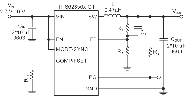
GUID-FD1A2092-6546-4309-911F-7B6A31779F43-low.gifSimplified Schematic
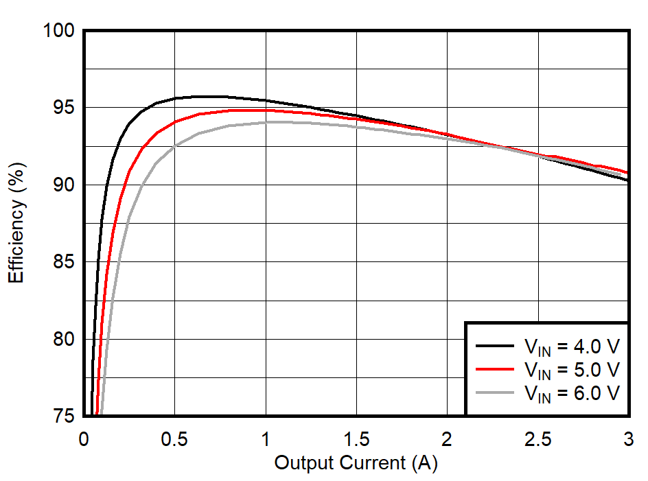
GUID-20210228-CA0I-C1XK-QHCZ-WH8H78MJXXPH-low.gifEfficiency Versus IOUT, VOUT = 3.3 V