SLVSGV4A October   2022  – March 2023 TPS62992-Q1

PRODUCTION DATA  

  1. Features
  2. Applications
  3. Description
  4. Revision History
  5. Device Comparison Table
  6. Pin Configuration and Functions
  7. Specifications
    1. 7.1 Absolute Maximum Ratings
    2. 7.2 ESD Ratings
    3. 7.3 Recommended Operating Conditions
    4. 7.4 Thermal Information
    5. 7.5 Electrical Characteristics
    6. 7.6 Typical Characteristics
  8. Detailed Description
    1. 8.1 Overview
    2. 8.2 Functional Block Diagram
    3. 8.3 Feature Description
      1. 8.3.1  Mode Selection and Device Configuration MODE/S-CONF
      2. 8.3.2  Adjustable VO Operation (External Voltage Divider)
      3. 8.3.3  Selectable VO Operation (VSET and Internal Voltage Divider)
      4. 8.3.4  Soft Start and Tracking (SS/TR)
        1. 8.3.4.1 Tracking Function
      5. 8.3.5  Smart Enable with Precise Threshold
      6. 8.3.6  Power Good (PG)
      7. 8.3.7  Output Discharge Function
      8. 8.3.8  Undervoltage Lockout (UVLO)
      9. 8.3.9  Current Limit and Short-Circuit Protection
      10. 8.3.10 High Temperature Specifications
      11. 8.3.11 Thermal Shutdown
    4. 8.4 Device Functional Modes
      1. 8.4.1 Forced Pulse Width Modulation (FPWM) Operation
      2. 8.4.2 Power Save Mode Operation (Auto PFM and PWM)
      3. 8.4.3 AEE (Automatic Efficiency Enhancement)
      4. 8.4.4 100% Duty-Cycle Operation
      5. 8.4.5 Starting into a Prebiased Load
  9. Application and Implementation
    1. 9.1 Application Information
    2. 9.2 Typical Application with Adjustable Output Voltage
      1. 9.2.1 Design Requirements
      2. 9.2.2 Detailed Design Procedure
        1. 9.2.2.1 Custom Design With WEBENCH® Tools
        2. 9.2.2.2 Programming the Output Voltage
        3. 9.2.2.3 External Component Selection
          1. 9.2.2.3.1 Output Filter and Loop Stability
          2. 9.2.2.3.2 Inductor Selection
          3. 9.2.2.3.3 Capacitor Selection
            1. 9.2.2.3.3.1 Output Capacitor
            2. 9.2.2.3.3.2 Input Capacitor
            3. 9.2.2.3.3.3 Soft-Start Capacitor
      3. 9.2.3 Application Curves
        1. 9.2.3.1 Application Curves Vout = 1.8 V
        2. 9.2.3.2 Application Curves Vout = 1.2 V
        3. 9.2.3.3 Application Curves Vout = 0.6 V
    3. 9.3 Typical Application with Selectable VOUT using VSET
      1. 9.3.1 Design Requirements
      2. 9.3.2 Detailed Design Procedure
        1. 9.3.2.1 Programming the Output Voltage
      3. 9.3.3 Application Curves
        1. 9.3.3.1 Application Curves Vout = 5 V
        2. 9.3.3.2 Application Curves Vout = 3.3 V
    4. 9.4 System Examples
      1. 9.4.1 LED Power Supply
      2. 9.4.2 Powering Multiple Loads
      3. 9.4.3 Voltage Tracking
      4. 9.4.4 Inverting Buck-Boost (IBB)
    5. 9.5 Power Supply Recommendations
    6. 9.6 Layout
      1. 9.6.1 Layout Guidelines
      2. 9.6.2 Layout Example
      3. 9.6.3 Thermal Considerations
  10. 10Device and Documentation Support
    1. 10.1 Device Support
      1. 10.1.1 Third-Party Products Disclaimer
      2. 10.1.2 Development Support
        1. 10.1.2.1 Custom Design With WEBENCH® Tools
    2. 10.2 Documentation Support
      1. 10.2.1 Related Documentation
    3. 10.3 Receiving Notification of Documentation Updates
    4. 10.4 Support Resources
    5. 10.5 Trademarks
    6. 10.6 Electrostatic Discharge Caution
    7. 10.7 Glossary
  11. 11Mechanical, Packaging, and Orderable Information

Package Options

Mechanical Data (Package|Pins)
Thermal pad, mechanical data (Package|Pins)
Orderable Information
Soft-Start Capacitor

A capacitor connected between SS/TR pin and GND allows a user-programmable start-up slope of the output voltage.
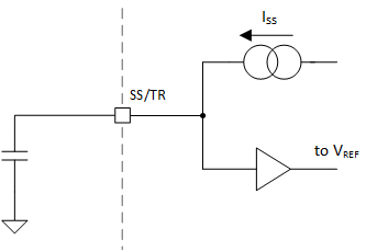
GUID-ACDCAE00-295F-4A45-8144-1191A3C18081-low.gifFigure 9-2 Soft-Start Operation Simplified Schematic

An internal constant current source is provided to charge the external capacitance. The capacitor required for a given soft-start ramp time is given by:

Equation 18. C S S = T S S × I S S V R E F

where

  • CSS is the capacitance required at the SS/TR pin.
  • TSS is the desired soft-start ramp time.
  • ISS is the SS/TR source current, see the Electrical Characteristics.
  • VREF is the feedback regulation voltage divided by tracking gain (VFB / 0.75); see the Electrical Characteristics.

The fastest achievable typical ramp time is 150 µs, even if the external Css capacitance is lower than 680 pF or the pin is open.