SLVSAM8D July 2013 – August 2019 TPS63050 , TPS63051
PRODUCTION DATA.
- 1 Features
- 2 Applications
- 3 Description
- 4 Revision History
- 5 Device Comparison Table
- 6 Pin Configuration and Functions
- 7 Specifications
- 8 Detailed Description
- 9 Application and Implementation
- 10Power Supply Recommendations
- 11Layout
- 12Device and Documentation Support
- 13Mechanical, Packaging, and Orderable Information
Package Options
Mechanical Data (Package|Pins)
Thermal pad, mechanical data (Package|Pins)
Orderable Information
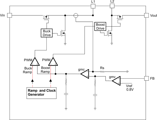
8.4.1 Control Loop Description
 Figure 6. Average Current Mode Control
 The controller circuit of the device is based on an average current mode topology. The average inductor current is regulated by a fast current regulator loop which is controlled by a voltage control loop. Figure 6 shows the control loop.
The noninverting input of the transconductance amplifier, gmv, is assumed to be constant. The output of gmv defines the average inductor current. The inductor current is reconstructed by measuring the current through the high side buck MOSFET. This current corresponds exactly to the inductor current in boost mode. In buck mode the current is measured during the on time of the same MOSFET. During the off time, the current is reconstructed internally starting from the peak value at the end of the on time cycle. The average current and the feedback from the error amplifier gmv forms the correction signal gmc. This correction signal is compared to the buck and the boost sawtooth ramp giving the PWM signal. Depending on which of the two ramps the gmc output crosses either the Buck or the Boost stage is initiated. When the input voltage is close to the output voltage, one buck cycle is always followed by a boost cycle. In this condition, no more than three cycles in a row of the same mode are allowed. This control method in the buck-boost region ensures a robust control and the highest efficiency.