SLVSC58B June   2016  – March 2019 TPS63070

PRODUCTION DATA.  

  1. Features
  2. Applications
  3. Description
    1.     Device Images
      1.      Simplified Schematic
      2.      Efficiency vs Output Current; Vo = 5 V
  4. Revision History
  5. Device Comparison Table
  6. Pin Configuration and Functions
    1.     Pin Functions
  7. Specifications
    1. 7.1 Absolute Maximum Ratings
    2. 7.2 ESD Ratings
    3. 7.3 Recommended Operating Conditions
    4. 7.4 Thermal Information
    5. 7.5 Electrical Characteristics
    6. 7.6 Typical Characteristics
  8. Detailed Description
    1. 8.1 Overview
    2. 8.2 Functional Block Diagram TPS63070
    3. 8.3 Functional Block Diagram TPS630701
    4. 8.4 Feature Description
      1. 8.4.1  Control Loop Description
      2. 8.4.2  Precise Enable
      3. 8.4.3  Power Good
      4. 8.4.4  Soft Start
      5. 8.4.5  PS/SYNC
      6. 8.4.6  Short Circuit Protection
      7. 8.4.7  VSEL and FB2 pins
      8. 8.4.8  Overvoltage Protection
      9. 8.4.9  Undervoltage Lockout
      10. 8.4.10 Overtemperature Protection
    5. 8.5 Device Functional Modes
      1. 8.5.1 Power Save Mode
      2. 8.5.2 Current Limit
      3. 8.5.3 Output Discharge Function (TPS630702 only)
  9. Application and Implementation
    1. 9.1 Application Information
    2. 9.2 Typical Application for adjustable version
      1. 9.2.1 Design Requirements
      2. 9.2.2 Detailed Design Procedure
        1. 9.2.2.1 Programming The Output Voltage
        2. 9.2.2.2 Inductor Selection
        3. 9.2.2.3 Capacitor Selection
          1. 9.2.2.3.1 Input Capacitor
          2. 9.2.2.3.2 Output Capacitor
      3. 9.2.3 Application Curves
    3. 9.3 Typical Application for Fixed Voltage Version
      1. 9.3.1 Design Requirements
      2. 9.3.2 Detailed Design Procedure
      3. 9.3.3 Application Curves
  10. 10Power Supply Recommendations
    1. 10.1 Thermal Information
  11. 11Layout
    1. 11.1 Layout Guidelines
    2. 11.2 Layout Example
  12. 12Device and Documentation Support
    1. 12.1 Device Support
      1. 12.1.1 Third-Party Products Disclaimer
    2. 12.2 Related Links
    3. 12.3 Receiving Notification of Documentation Updates
    4. 12.4 Community Resources
    5. 12.5 Trademarks
    6. 12.6 Electrostatic Discharge Caution
    7. 12.7 Glossary
  13. 13Mechanical, Packaging, and Orderable Information

Package Options

Mechanical Data (Package|Pins)
Thermal pad, mechanical data (Package|Pins)
Orderable Information

VSEL and FB2 pins

The VSEL pin allows to dynamically select between two different output voltages on the adjustable version. The voltage is set by a resistor that is connected between the FB and the FB2 pin. FB2 is connected to GND if VSEL = high. FB2 is high impedance if VSEL= low. The transition speed during a voltage change is defined by the loop bandwidth of the device and can be adjusted by adding a feed-forward capacitor in parallel to R1.
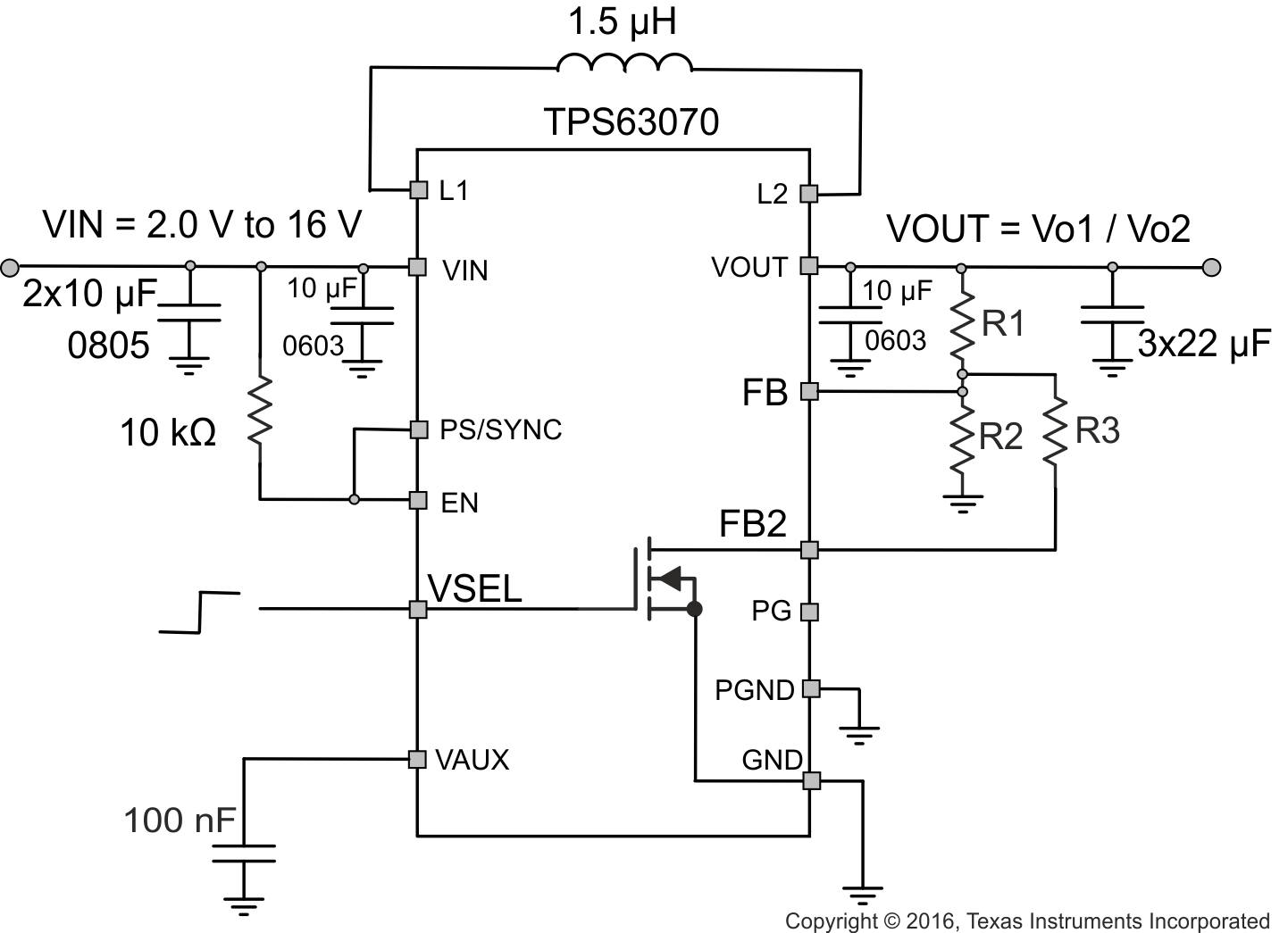
TPS63070 TPS63070_VSELonly_noILIM_SS.gifFigure 8. Typical Application using VSEL

The resistor values for the feedback divider and FB2 are in the 50-500kΩ range. R3 is calculated as follows:

Equation 1. TPS63070 Equation_new.gif

For more details on how to use VSEL see Technote SLVAE62.