SLVSDS9E July 2018 – August 2021 TPS63805 , TPS63806 , TPS63807
PRODUCTION DATA
- 1 Features
- 2 Applications
- 3 Description
- 4 Revision History
- 5 Description (continued)
- 6 Device Comparison Table
- 7 Pin Configuration and Functions
- 8 Specifications
-
9 Detailed Description
- 9.1 Overview
- 9.2 Functional Block Diagram
- 9.3
Feature Description
- 9.3.1 Control Loop Description
- 9.3.2 Precise Device Enable: Threshold- or Delayed Enable
- 9.3.3 Mode Selection (PFM/PWM)
- 9.3.4 Undervoltage Lockout (UVLO)
- 9.3.5 Soft Start
- 9.3.6 Adjustable Output Voltage
- 9.3.7 Overtemperature Protection - Thermal Shutdown
- 9.3.8 Input Overvoltage - Reverse-Boost Protection (IVP)
- 9.3.9 Output Overvoltage Protection (OVP)
- 9.3.10 Power-Good Indicator
- 9.4 Device Functional Modes
- 10Application and Implementation
- 11Power Supply Recommendations
- 12Layout
- 13Device and Documentation Support
- 14Mechanical, Packaging, and Orderable Information
Package Options
Mechanical Data (Package|Pins)
- YFF|15
Thermal pad, mechanical data (Package|Pins)
Orderable Information
9.4.1.1 Reverse Current Operation, Negative Current
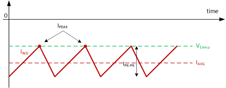
When the TPS63805, TPS63806, and TPS63807 are forced to PWM operation (MODE = HIGH), the device current can flow in reverse direction. This happens by the negative current capability of the TPS63805, TPS63806, and TPS63807. The error amplifier provides a peak-current target (voltage that is translated into an equivalent current, see Figure 9-1), even if the target has a negative value. The maximum average current is even more negative than the peak current.
 Figure 9-6 Peak-Current Operation, Reverse Current