SLVS496D SEPTEMBER 2003 – August 2016 TPS65100 , TPS65101 , TPS65105
PRODUCTION DATA.
- 1 Features
- 2 Applications
- 3 Description
- 4 Revision History
- 5 Device Options
- 6 Pin Configuration and Functions
- 7 Specifications
- 8 Detailed Description
- 9 Application and Implementation
- 10Power Supply Recommendations
- 11Layout
- 12Device and Documentation Support
- 13Mechanical, Packaging, and Orderable Information
Package Options
Refer to the PDF data sheet for device specific package drawings
Mechanical Data (Package|Pins)
- RGE|24
- PWP|24
Thermal pad, mechanical data (Package|Pins)
Orderable Information
11 Layout
11.1 Layout Guidelines
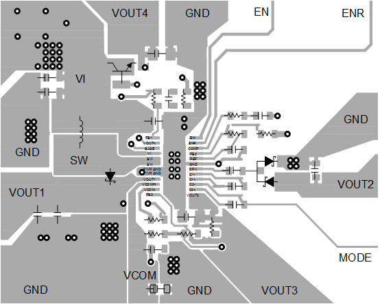
For all switching power supplies, the layout is an important step in the design, especially at high-peak currents and switching frequencies. If the layout is not carefully designed, the regulator might show stability and EMI problems. Therefore, the traces carrying high-switching currents should be routed first using wide and short traces. The input filter capacitor should be placed as close as possible to the input pin VIN of the IC. TI recommends the following PCB layout guidelines for the TPS6510x devices:
- Connect PGND and AGND together on the same ground plane
- Connect all capacitor grounds and PGND together on a common ground plane.
- Place the input capacitor as close as possible to the input pin of the IC.
- Place the rectifier diode as close as possible to the IC
- Route first the traces carrying high-switching current with wide and short traces
- Isolate analog signal paths from power paths.
- If vias are necessary, try to use more than one in parallel to decrease parasitics, especially for power traces.
- Solder the thermal pad to the PCB for good thermal performance.
11.2 Layout Example
 Figure 21. TPS6510x Layout Example
11.3 Thermal Performance
An influential component of thermal performance of a package is board design. To take full advantage of the heat dissipation abilities of the PowerPAD or VQFN package with exposed thermal die, a board that acts similar to a heat sink and allows the use of an exposed (and solderable) deep downset pad should be used. For further information, see the Texas Instruments application notes PowerPAD Thermally Enhanced Package and PowerPAD Made Easy. For the VQFN package, see the QFN/SON PCB Attachement application report. Especially for the VQFN package it is required to solder down the Thermal Pad to achieve the required thermal resistance.