SLVS704C November 2011 – January 2017 TPS65135
PRODUCTION DATA.
- 1 Features
- 2 Applications
- 3 Description
- 4 Revision History
- 5 Pin Configuration and Functions
- 6 Specifications
- 7 Detailed Description
- 8 Application and Implementation
- 9 Power Supply Recommendations
- 10Layout
- 11Device and Documentation Support
- 12Mechanical, Packaging, and Orderable Information
Package Options
Mechanical Data (Package|Pins)
- RTE|16
Thermal pad, mechanical data (Package|Pins)
- RTE|16
Orderable Information
1 Features
- Single-Inductor, Multiple-Output Topology
- 2.5-V to 5.5-V Input Voltage Range
- 750-mW Output Power at VI = 2.9 V
- Positive Output Voltages Up to 6 V
- Negative Output Voltage Down to –7 V
- 1% Output Voltage Accuracy
- Up to 50% Output Current Mismatch Allowed
- Excellent Line Regulation
- Advanced Power-Save Mode for Light-Load
Efficiency - Low-Noise Operation
- Out-of-Audio Mode
- Short-Circuit Protection
- Thermal Shutdown
- 3-mm × 3-mm Thin QFN Package
2 Applications
- AMOLED Display Power Supplies
- LCD Power Supplies
- Split-Rail Power Supplies for Op-Amps, Data Converters, Data Interfaces, etc.
3 Description
The TPS65135 device is a high-efficiency split-rail power supply. Thanks to its single-inductor, multiple-output (SIMO) topology, the converter uses very few external components. The device operates with a buck-boost topology and generates positive and negative output voltages above or below the input supply voltage. The SIMO topology achieves excellent line and load regulation, which is necessary, for example, to avoid disturbance of a mobile phone display as a result of input voltage variations that occur during transmit periods in mobile communication systems. The device can also be used as a general-purpose split-rail supply as long as the output current mismatch between the rails is less than 50%.
Device Information(1)
| PART NUMBER | PACKAGE | BODY SIZE (NOM) |
|---|---|---|
| TPS65135 | WQFN (16) | 3.00 mm × 3.00 mm |
- For all available packages, see the orderable addendum at the end of the data sheet.
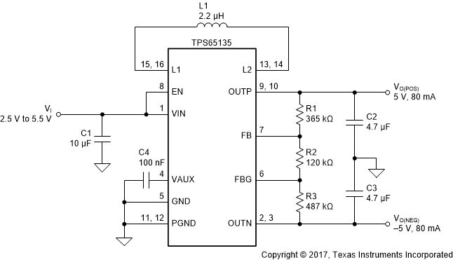
Typical Application Schematic
