SLVSBG2A September   2013  – June 2016 TPS65154

PRODUCTION DATA.  

  1. Device Overview
    1. 1.1 Features
    2. 1.2 Applications
    3. 1.3 Description
    4. 1.4 Simplified System Diagram
  2. Revision History
  3. Pin Configuration and Functions
  4. Specifications
    1. 4.1 Absolute Maximum Ratings
    2. 4.2 ESD Ratings
    3. 4.3 Recommended Operating Conditions
    4. 4.4 Thermal Information
    5. 4.5 Electrical Characteristics
    6. 4.6 Timing Requirements
  5. Detailed Description
    1. 5.1 Overview
    2. 5.2 Functional Block Diagram
    3. 5.3 Feature Description
      1. 5.3.1  Linear Regulator (VCC)
        1. 5.3.1.1 Power-Up (Linear Regulator)
        2. 5.3.1.2 Power-Down (Linear Regulator)
        3. 5.3.1.3 Protection (Linear Regulator)
      2. 5.3.2  Boost Converter 1 (AVDD)
        1. 5.3.2.1 Power-Up (Boost Converter 1)
        2. 5.3.2.2 Power-Down (Boost Converter 1)
        3. 5.3.2.3 Protection (Boost Converter 1)
      3. 5.3.3  Boost Converter 2 (VGH)
        1. 5.3.3.1 Power-Up (Boost Converter 2)
        2. 5.3.3.2 Power-Down (Boost Converter 2)
        3. 5.3.3.3 Protection (Boost Converter 2)
      4. 5.3.4  Negative Charge Pump (VGL)
        1. 5.3.4.1 Power-Up (Negative Charge Pump)
        2. 5.3.4.2 Power-Down (Negative Charge Pump)
        3. 5.3.4.3 Protection (Negative Charge Pump)
      5. 5.3.5  Gate Voltage Shaping
      6. 5.3.6  Panel Discharge (XAO)
      7. 5.3.7  Reset Generator (RST)
      8. 5.3.8  Programmable VCOM
        1. 5.3.8.1 Operational Amplifier Performance
        2. 5.3.8.2 Power-Up (Programmable VCOM)
        3. 5.3.8.3 Power-Down (Programmable VCOM)
      9. 5.3.9  WLED Driver
        1. 5.3.9.1 WLED Boost Converter
        2. 5.3.9.2 Current Sinks
        3. 5.3.9.3 Protection
        4. 5.3.9.4 Enable and Start-Up
      10. 5.3.10 Undervoltage Lockout
    4. 5.4 Device Functional Modes
      1. 5.4.1 Dimming Modes
        1. 5.4.1.1 Direct Dimming
        2. 5.4.1.2 Phase-Shift Dimming
      2. 5.4.2 Power Sequencing
        1. 5.4.2.1 Power-Up
        2. 5.4.2.2 Power-Down
    5. 5.5 Programming
      1. 5.5.1 Configuration
        1. 5.5.1.1 General
          1. 5.5.1.1.1 I2C Interface
          2. 5.5.1.1.2 Slave Addresses
          3. 5.5.1.1.3 Write Protect
      2. 5.5.2 Programming Examples (Excluding VCOM)
        1. 5.5.2.1 Writing to a Single RAM Register
        2. 5.5.2.2 Writing to Multiple RAM Registers
        3. 5.5.2.3 Saving Contents of all RAM Registers to EEPROM
        4. 5.5.2.4 Reading from a Single RAM Register
        5. 5.5.2.5 Reading from a Single EEPROM Register
        6. 5.5.2.6 Reading from Multiple RAM Registers
        7. 5.5.2.7 Reading from Multiple EEPROM Registers
      3. 5.5.3 Programming Examples - VCOM
        1. 5.5.3.1 Writing a VCOM Value of 77h to WR
        2. 5.5.3.2 Writing a VCOM Value of 77h to IVR and WR
        3. 5.5.3.3 Reading a VCOM Value of 77h from WR
        4. 5.5.3.4 Reading a VCOM Value of 77h from IVR
    6. 5.6 Register Map
      1. 5.6.1 Configuration Registers (Excluding VCOM)
        1. 5.6.1.1  CONFIG (00h)
        2. 5.6.1.2  VCC (01h)
        3. 5.6.1.3  DLY1 (02h)
        4. 5.6.1.4  AVDD (03h)
        5. 5.6.1.5  FSW1 (04h)
        6. 5.6.1.6  SS2 (05h)
        7. 5.6.1.7  DLY2 (06h)
        8. 5.6.1.8  VGL (07h)
        9. 5.6.1.9  SS3 (08h)
        10. 5.6.1.10 DLY3 (09h)
        11. 5.6.1.11 VGH (0Ah)
        12. 5.6.1.12 SS4 (0Bh)
        13. 5.6.1.13 FSW3 (0Ch)
        14. 5.6.1.14 DLY4 (0Dh)
        15. 5.6.1.15 OVP (0Eh)
        16. 5.6.1.16 FDIM (OFh)
        17. 5.6.1.17 RESET (10h)
        18. 5.6.1.18 VDET (11h)
        19. 5.6.1.19 DLY6 (12h)
        20. 5.6.1.20 VMAX (13h)
        21. 5.6.1.21 VMIN (14h)
        22. 5.6.1.22 USER (15h)
        23. 5.6.1.23 CONTROL (FFh)
      2. 5.6.2 VCOM Registers
        1. 5.6.2.1 VCOM DATA (Slave Address 28h, Register Address 00h)
        2. 5.6.2.2 VCOM CONTROL (Slave Address 28h, Register Address 02h)
  6. Application and Implementation
    1. 6.1 Application Information
    2. 6.2 Typical Application
      1. 6.2.1 Design Requirements
      2. 6.2.2 Detailed Design Procedure
        1. 6.2.2.1 External Component Selection
      3. 6.2.3 Application Curves
  7. Power Supply Recommendations
  8. Layout
    1. 8.1 Layout Guidelines
    2. 8.2 Layout Example
  9. Device and Documentation Support
    1. 9.1 Device Support
      1. 9.1.1 Third-Party Products Disclaimer
    2. 9.2 Receiving Notification of Documentation Updates
    3. 9.3 Community Resources
    4. 9.4 Trademarks
    5. 9.5 Electrostatic Discharge Caution
    6. 9.6 Glossary
  10. 10Mechanical, Packaging, and Orderable Information
    1. 10.1 Packaging Information

Package Options

Mechanical Data (Package|Pins)
Thermal pad, mechanical data (Package|Pins)
Orderable Information

6 Application and Implementation

NOTE

Information in the following Applications section is not part of the TI component specification, and TI does not warrant its accuracy or completeness. TI's customers are responsible for determining suitability of components for their purposes. Customers should validate and test their design implementation to confirm system functionality.

6.1 Application Information

The TPS65154 devices is intended primarily for use in notebook PC and tablet applications. It needs these two supply voltages

  • A regulated 3.3-V or 5-V supply for the LCD bias functions
  • A direct connection to the battery for the WLED driver functions

The device configuration parameters are set by I2C interface and stored in the on-chip nonvolatile memory.

6.2 Typical Application

Figure 6-1 shows the recommended application circuit for typical applications. The I2C interface is used to optimize the circuit's operating parameters for a specific application. If different component values are used, make sure that the values are within the recommended operating conditions (see Recommended Operating Conditions). If different component values are used, the compensation components may also need to be optimized for stability and best performance.
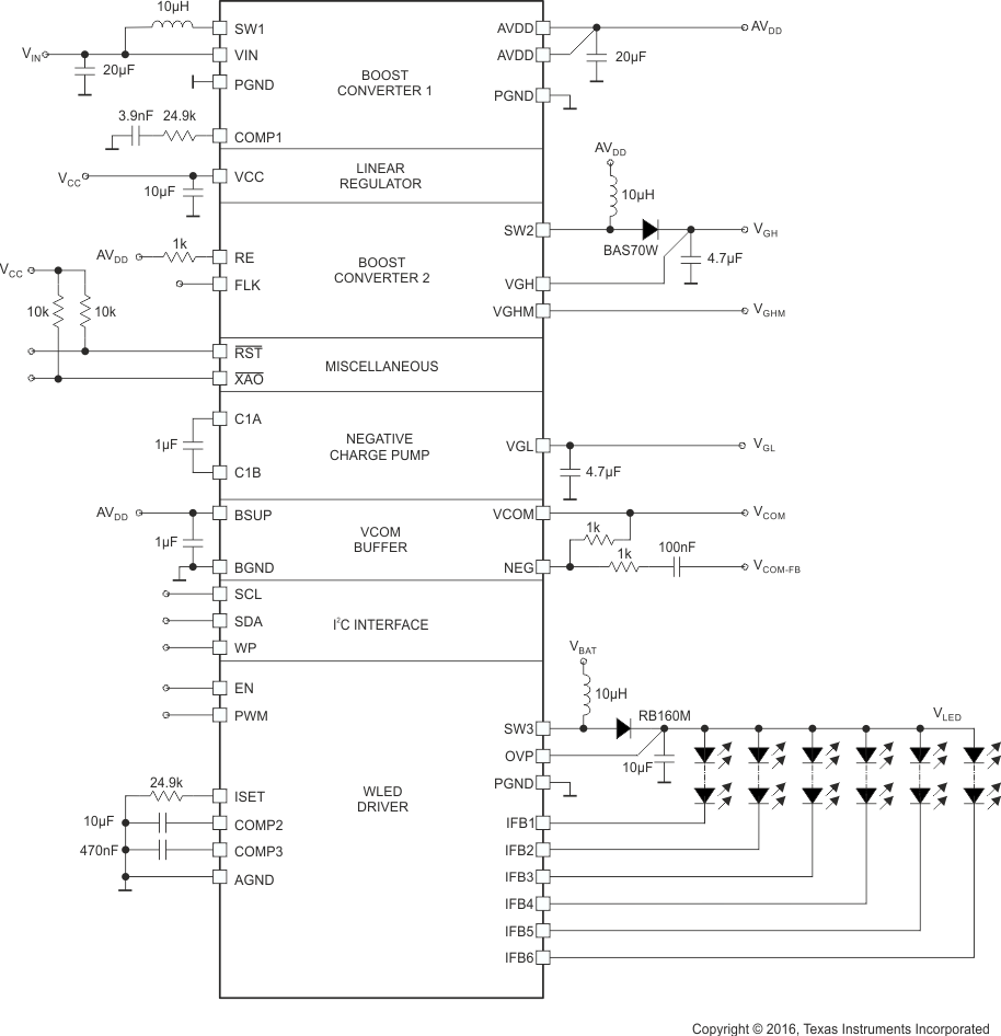
TPS65154 G601_SLVSBG2.gif Figure 6-1 Typical Application Circuit

6.2.1 Design Requirements

This design example uses the parameters listed in Table 6-1 as the input parameters.

Table 6-1 Input Parameters

PARAMETER SYMBOL VALUE
Input supply voltage – LCD bias functions VIN 3.3 V
Input supply voltage – WLED driver VBAT 9 V to 21 V
Boost converter 1 output voltage AVDD 8 V
Inverting charge pump output voltage VGL –6.8 V
Boost converter 2 output voltage VGH 20 V
Linear regulator output voltage VCC 2.5 V
WLED driver output current (per string) ISET 50 mA

6.2.2 Detailed Design Procedure

6.2.2.1 External Component Selection

Care should be applied to the choice of external components since they greatly affect overall performance. The TPS65154 was developed with the twin goals of high performance and small/low-profile solution size. Since these two goals are often in direct opposition to one another (for example, larger inductors tend to achieve higher efficiencies), some trade-off is always necessary.

Inductors must have adequate current capability so that they do not saturate under worst-case conditions. For high efficiency, they should also have low dc resistance (DCR).

Capacitors must have adequate effective capacitance under the applicable dc bias conditions they experience in the application. MLCC capacitors typically exhibit only a fraction of their nominal capacitance under real-world conditions and this must be taken into consideration when selecting them. This problem is especially acute in low profile capacitors, in which the dielectric field strength is higher than in taller components. In general, the capacitance values shown in circuit diagrams in this data sheet refer to the effective capacitance after dc bias effects have been taken into consideration. Reputable capacitor manufacturers provide capacitance versus dc bias curves that greatly simplify component selection.

The following tables list some components suitable for use with the TPS65154. The list is not exhaustive – other components may exist that are equally suitable (or better), however, these components have been proven to work well and were used extensively during the development of the TPS65154.

Table 6-2 Linear Regulator External Component Recommendations

REF. DESCRIPTION PART NUMBER MANUFACTURER MAX. THICKNESS
COUT 10 µF, 6.3 V, ±20%, X5R, 0603 GRM188R60J106ME84 Murata 0.95 mm

Table 6-3 Boost Converter 1 External Components

REF. DESCRIPTION PART NUMBER MANUFACTURER MAX. THICKNESS
L 10 µH, 1.5 A, 0.205 Ω NRS6012T100MMGG Taiyo Yuden 1.2 mm
COUT 10 µF, 16 V, ±10%, X5R, 1206 GRM319R61C106KE15D Murata 0.85 ±0.1 mm

Table 6-4 Boost Converter 2 External Components

REF. DESCRIPTION PART NUMBER MANUFACTURER MAX. THICKNESS
L 10 µH, 0.6 A NRH3010T100MN Taiyo Yuden 1 mm
COUT 4.7 µF, 50 V, ±10%, X5R, 1206 GRM319R61H475KA12 Murata 0.95 mm

Table 6-5 Boost Converter 3 External Components

REF. DESCRIPTION PART NUMBER MANUFACTURER MAX. THICKNESS
L 10 µH, 1.5 A, 0.205 Ω NRS6012T100MMGGJ Taiyo Yuden 1.2 mm
COUT 4.7 µF, 50 V, ±10%, X5R, 1206 GRM319R61H475KA12 Murata 0.95 mm

6.2.3 Application Curves
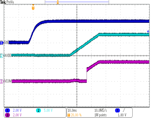
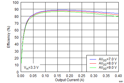
TPS65154 G401_SLVSBG2.png
Figure 6-2 Boost Converter 1 (AVDD) Efficiency
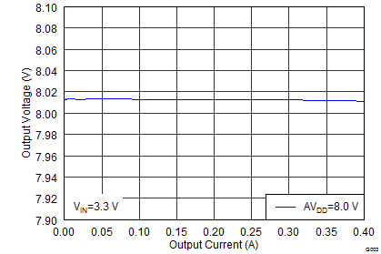
TPS65154 G403_SLVSBG2.png
Figure 6-4 Boost Converter 1 (AVDD) Load Regulation
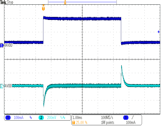
TPS65154 G405_SLVSBG2.gif
Figure 6-6 Boost Converter 1 (AVDD) Load Transient Response
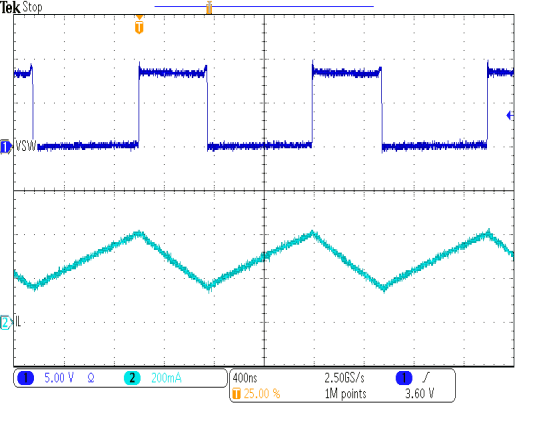
TPS65154 G407_SLVSBG2.gif
Figure 6-8 Boost Converter 1 (AVDD) Switching Waveforms
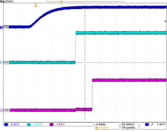
TPS65154 G409_SLVSBG2.png
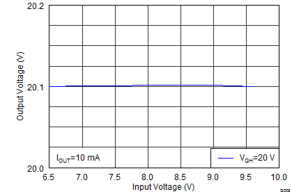
Figure 6-10 Boost Converter 2 (VGH) Line Regulation
TPS65154 G411_SLVSBG2.gif
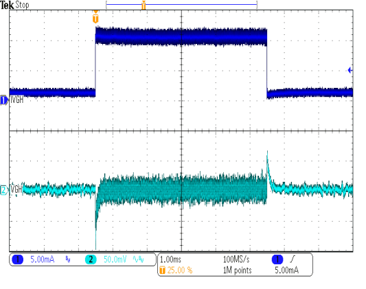
Figure 6-12 Boost Converter 2 (VGH) Load Transient Response
TPS65154 G413_SLVSBG2.gif
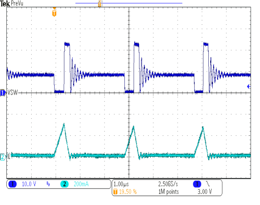
Figure 6-14 Boost Converter 2 (VGH) Switching Waveforms
TPS65154 G415_SLVSBG2.png
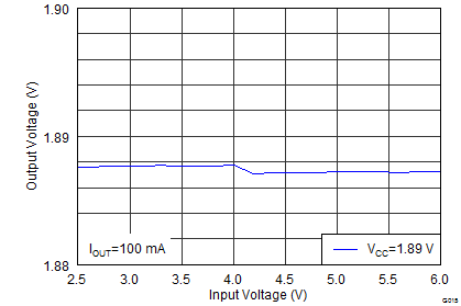
Figure 6-16 Linear Regulator (VCC) Line Regulation
TPS65154 G417_SLVSBG2.gif
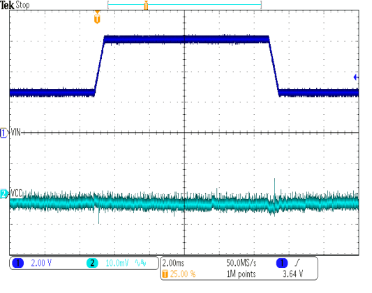
Figure 6-18 Linear Regulator (VCC) Line Transient Response
TPS65154 G419_SLVSBG2.png
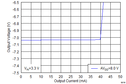
Figure 6-20 Negative Charge Pump (VGL) Load Regulation
TPS65154 G421_SLVSBG2.gif
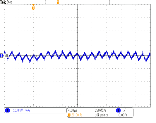
Figure 6-22 Negative Charge Pump (VGL) Output Voltage Ripple
TPS65154 G423_SLVSBG2.gif
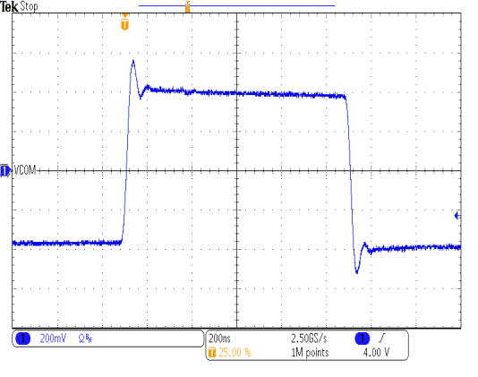
Figure 6-24 VCOM Buffer Large-Signal Response
TPS65154 G425_SLVSBG2.gif
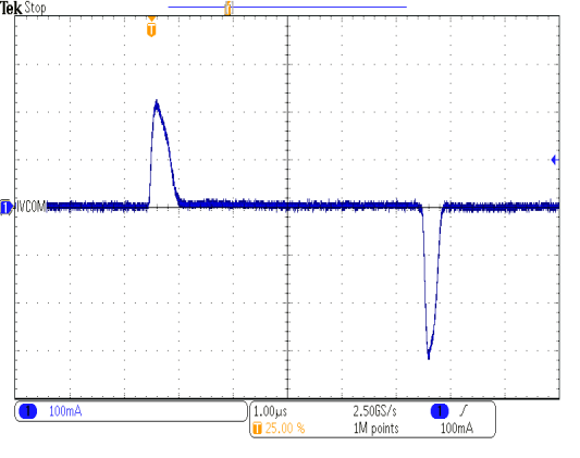
Figure 6-26 VCOM Buffer Peak Output Current
TPS65154 G427_SLVSBG2.gif
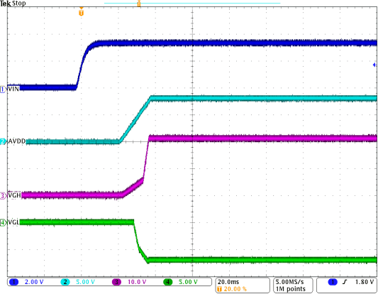
Figure 6-28 LCD Bias Power-Up Sequencing
TPS65154 G429_SLVSBG2.gif
Figure 6-30 LCD Bias Power-Up Sequencing
TPS65154 G431_SLVSBG2.gif
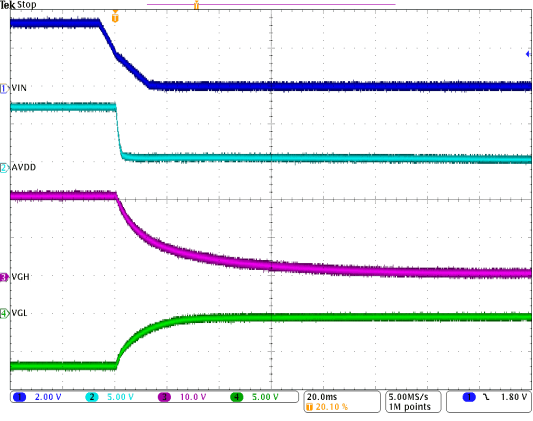
Figure 6-32 LCD Bias Power-Down Sequencing
TPS65154 G433_SLVSBG2.gif
Figure 6-34 LCD Bias Power-Down Sequencing
TPS65154 G435_SLVSBG2.png
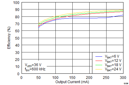
Figure 6-36 Boost Converter 3 (VLED) Efficiency
TPS65154 G437_SLVSBG2.png
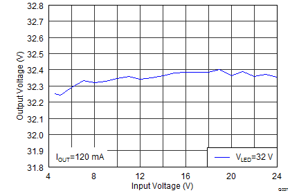
Figure 6-38 Boost Converter 3 (VLED) Line Regulation
TPS65154 G439_SLVSBG2.gif
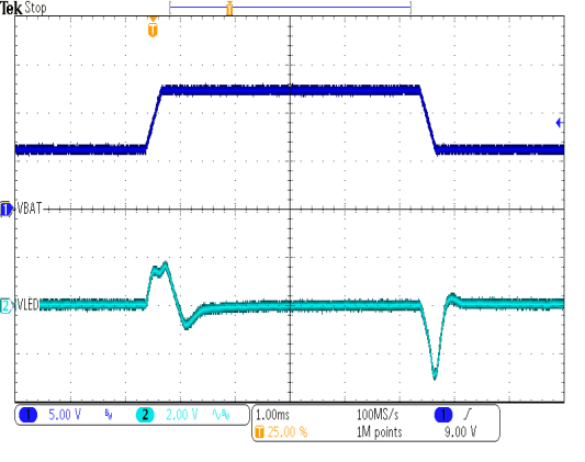
Figure 6-40 Boost Converter 3 (VLED) Line Transient Response
TPS65154 G441_SLVSBG2.gif
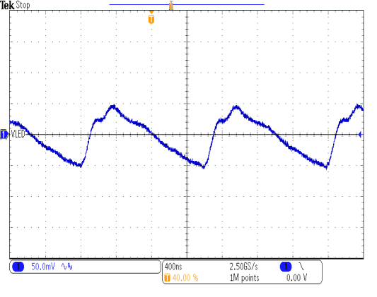
Figure 6-42 Boost Converter 3 (VLED) Output Voltage Ripple
TPS65154 G443_SLVSBG2.gif
Figure 6-44 PWM Direct Dimming Waveforms
TPS65154 G445_SLVSBG2.gif
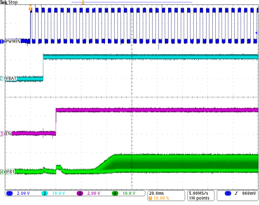
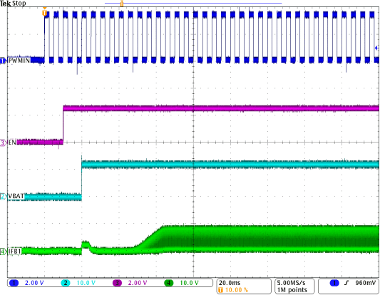
Figure 6-46 WLED Driver Power-Up Sequence
TPS65154 G447_SLVSBG2.gif
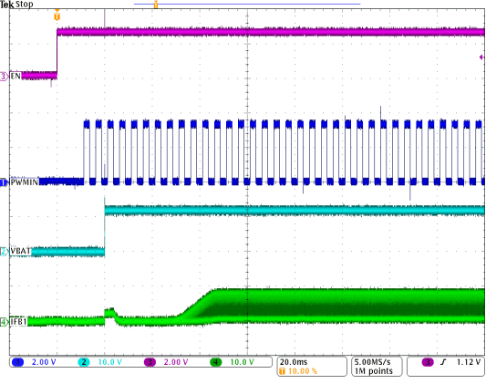
Figure 6-48 WLED Driver Power-Up Sequence
TPS65154 G449_SLVSBG2.gif
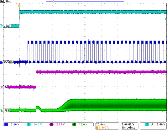
Figure 6-50 WLED Driver Power-Up Sequence
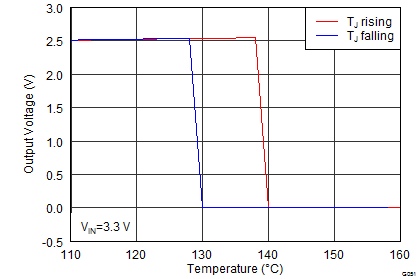
TPS65154 G451_SLVSBG2.png
Figure 6-52 Thermal Shutdown
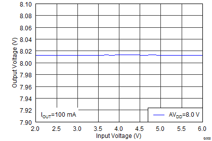
TPS65154 G402_SLVSBG2.png
Figure 6-3 Boost Converter 1 (AVDD) Line Regulation
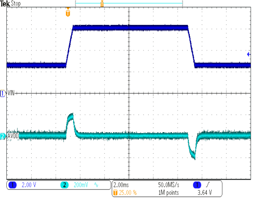
TPS65154 G404_SLVSBG2.gif
Figure 6-5 Boost Converter 1 (AVDD) Line Transient Response
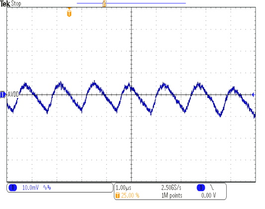
TPS65154 G406_SLVSBG2.gif
Figure 6-7 Boost Converter 1 (AVDD) Output Voltage Ripple
TPS65154 G408_SLVSBG2.png
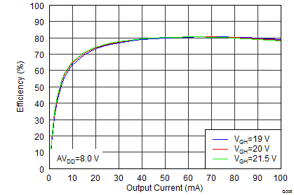
Figure 6-9 Boost Converter 2 (VGH) Efficiency
TPS65154 G410_SLVSBG2.png
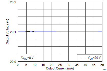
Figure 6-11 Boost Converter 2 (VGH) Load Regulation
TPS65154 G412_SLVSBG2.gif
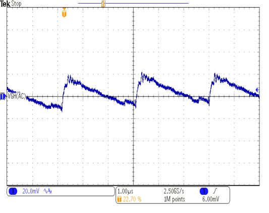
Figure 6-13 Boost Converter 2 (VGH) Output Voltage Ripple
TPS65154 G414_SLVSBG2.png
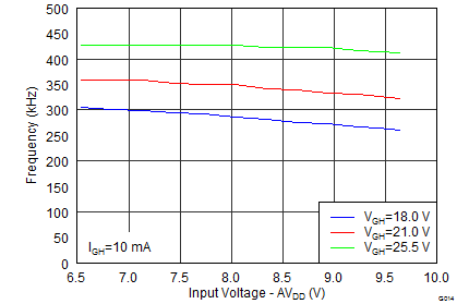
Figure 6-15 Boost Converter 2 (VGH) Switching Frequency
TPS65154 G416_SLVSBG2.png
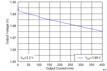
Figure 6-17 Linear Regulator (VCC) Load Regulation
TPS65154 G418_SLVSBG2.gif
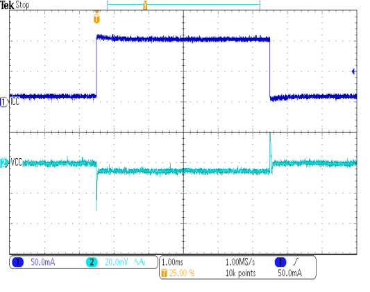
Figure 6-19 Linear Regulator (VCC) Load Transient Response
TPS65154 G420_SLVSBG2.gif
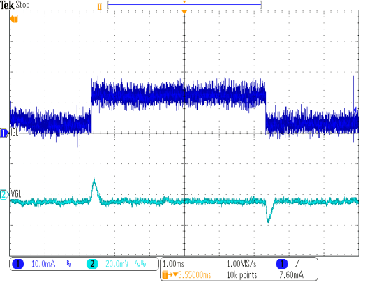
Figure 6-21 Negative Charge Pump (VGL) Load Transient Response
TPS65154 G422_SLVSBG2.gif
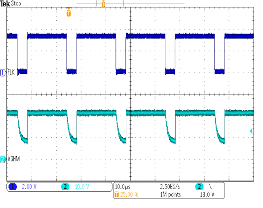
Figure 6-23 Gate Voltage Shaping (VGHM) Switching Waveforms
TPS65154 G424_SLVSBG2.gif
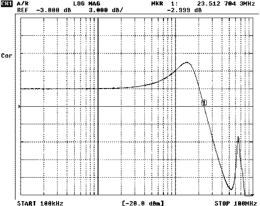
Figure 6-25 VCOM Buffer Small-Signal Bandwidth
TPS65154 G426_SLVSBG2.gif
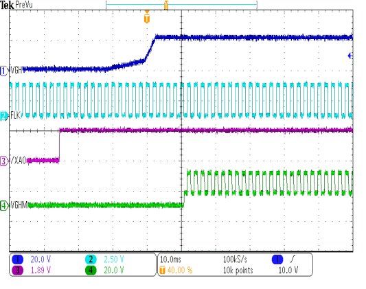
Figure 6-27 LCD Bias Power-Up Sequencing
TPS65154 G428_SLVSBG2.gif
Figure 6-29 LCD Bias Power-Up Sequencing
TPS65154 G430_SLVSBG2.gif
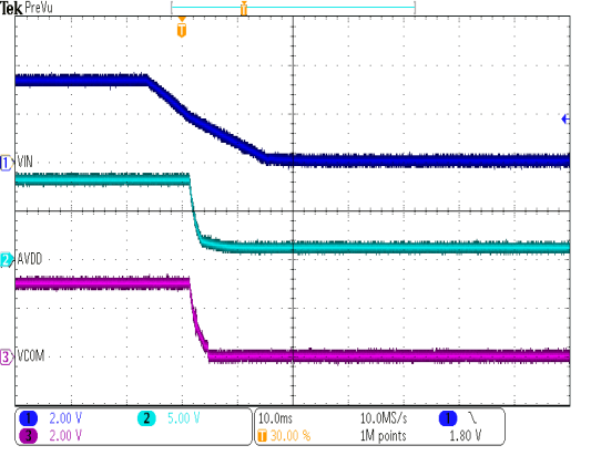
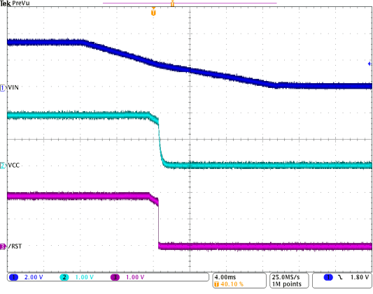
Figure 6-31 LCD Bias Power-Down Sequencing
TPS65154 G432_SLVSBG2.gif
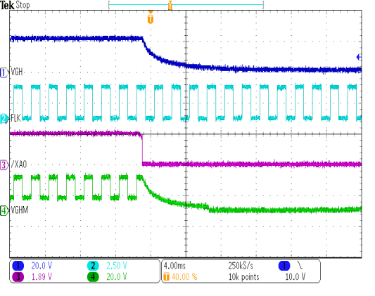
Figure 6-33 LCD Bias Power-Down Sequencing
TPS65154 G433_SLVSBG2.gif
Figure 6-35 Boost Converter 3 (VLED) Efficiency
TPS65154 G436_SLVSBG2.png
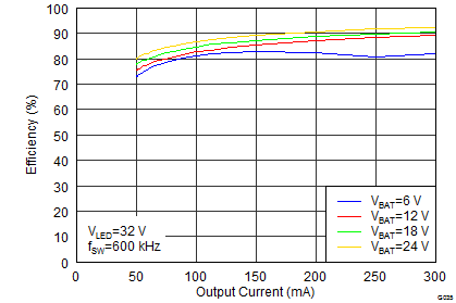
Figure 6-37 Boost Converter 3 (VLED) Efficiency
TPS65154 G438_SLVSBG2.png
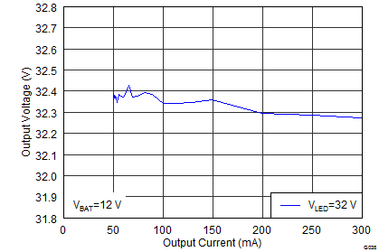
Figure 6-39 Boost Converter 3 (VLED) Load Regulation
TPS65154 G440_SLVSBG2.gif
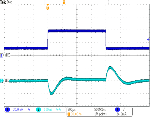
Figure 6-41 Boost Converter 3 (VLED) Load Transient Response
TPS65154 G442_SLVSBG2.gif
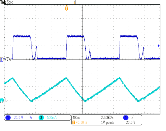
Figure 6-43 Boost Converter 3 (VLED) Switching Waveforms
TPS65154 G444_SLVSBG2.gif
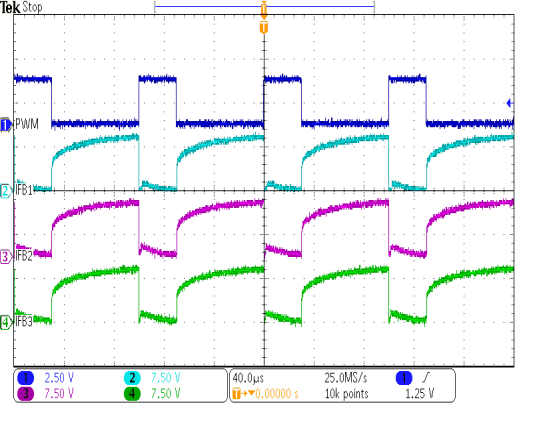
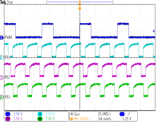
Figure 6-45 PWM Phase-Shifted Dimming
TPS65154 G446_SLVSBG2.gif
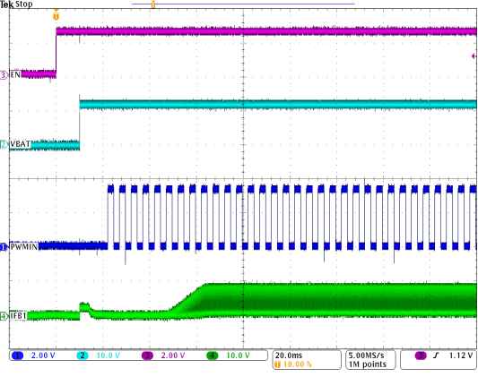
Figure 6-47 WLED Driver Power-Up Sequence
TPS65154 G448_SLVSBG2.gif
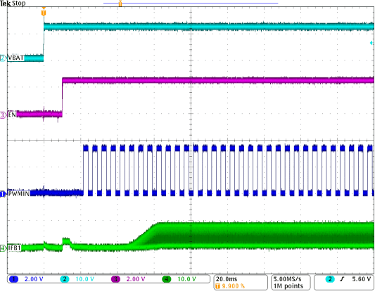
Figure 6-49 WLED Driver Power-Up Sequence
TPS65154 G450_SLVSBG2.gif
Figure 6-51 WLED Driver Power-Up Sequence