SLVSD80D November 2015 – May 2021 TPS65235
PRODUCTION DATA
- 1 Features
- 2 Applications
- 3 Description
- 4 Revision History
- 5 Pin Configuration and Functions
- 6 Specifications
-
7 Detailed Description
- 7.1 Overview
- 7.2 Functional Block Diagram
- 7.3
Feature Description
- 7.3.1 Boost Converter
- 7.3.2 Linear Regulator and Current Limit
- 7.3.3 Boost Converter Current Limit
- 7.3.4 Charge Pump
- 7.3.5 Slew Rate Control
- 7.3.6 Short Circuit Protection, Hiccup and Overtemperature Protection
- 7.3.7 Tone Generation
- 7.3.8 Tone Detection
- 7.3.9 Disable and Enable
- 7.3.10 Component Selection
- 7.4 Device Functional Modes
- 7.5 Programming
- 7.6 Register Maps
- 8 Application and Implementation
- 9 Power Supply Recommendations
- 10Layout
- 11Device and Documentation Support
- 12Mechanical, Packaging, and Orderable Information
Package Options
Mechanical Data (Package|Pins)
- RUK|20
Thermal pad, mechanical data (Package|Pins)
- RUK|20
Orderable Information
7.3.2 Linear Regulator and Current Limit
The linear regulator is used to generate the 22-kHz tone signal by changing the LDO reference voltage. The linear regulator features low drop out voltage to minimize power loss while keeps enough head room for the 22-kHz tone with 650-mV amplitude. It also implements a tight current limit for overcurrent protection. The current limit is set by an external resistor connected to ISET pin. Figure 7-1 shows the relationship between the current limit threshold and the resistor value.
 Figure 7-1 Linear Regulator Current Limit Vs Resistor
Equation 1. 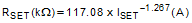
A 200-kΩ resistor sets the current to be 0.65 A, and 110-kΩ resistor sets the current to approximately 1 A.