SLVSC70B January 2015 – January 2022 TPS65251-1 , TPS65251-2 , TPS65251-3
PRODUCTION DATA
- 1 Features
- 2 Applications
- 3 Description
- 4 Revision History
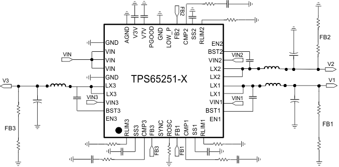
- 5 Pin Configuration and Functions
- 6 Specifications
-
7 Detailed Description
- 7.1 Overview
- 7.2 Functional Block Diagram
- 7.3
Feature Description
- 7.3.1 Adjustable Switching Frequency
- 7.3.2 Synchronization
- 7.3.3 Out-of-Phase Operation
- 7.3.4 Delayed Start-Up
- 7.3.5 Soft-Start Time
- 7.3.6 Adjusting the Output Voltage
- 7.3.7 Input Capacitor
- 7.3.8 Bootstrap Capacitor
- 7.3.9 Error Amplifier
- 7.3.10 Slope Compensation
- 7.3.11 Power Good
- 7.3.12 3.3-V and 6.5-V LDO Regulators
- 7.3.13 Current Limit Protection
- 7.3.14 Overvoltage Transient Protection (OVP)
- 7.3.15 Thermal Shutdown
- 7.4 Device Functional Modes
-
8 Application and Implementation
- 8.1 Application Information
- 8.2
Typical Application
- 8.2.1 Design Requirements
- 8.2.2
Detailed Design Procedure
- 8.2.2.1 Loop Compensation Circuit
- 8.2.2.2 Selecting the Switching Frequency
- 8.2.2.3 Output Inductor Selection
- 8.2.2.4 Output Capacitor
- 8.2.2.5 Input Capacitor
- 8.2.2.6 Soft-Start Capacitor
- 8.2.2.7 Bootstrap Capacitor Selection
- 8.2.2.8 Adjustable Current Limiting Resistor Selection
- 8.2.2.9 Output Voltage and Feedback Resistors Selection
- 8.2.2.10 Compensation
- 8.2.2.11 3.3-V and 6.5-V LDO Regulators
- 8.2.3 Application Curves
- 9 Power Supply Recommendations
- 10Layout
- 11Device and Documentation Support
- 12Mechanical, Packaging, and Orderable Information
Package Options
Mechanical Data (Package|Pins)
- RHA|40
Thermal pad, mechanical data (Package|Pins)
- RHA|40
Orderable Information
3 Description
The TPS65251-x features three synchronous wide-input range, high-efficiency buck converters. The converters are designed to simplify its application while giving the designer the option to optimize their usage according to the target application.
The converters can operate in 5-, 9-, 12- or 15-V systems and have integrated power transistors. The output voltage can be set externally using a resistor divider to any value between 0.8 V and close to the input supply. Each converter features an enable pin that allows a delayed start-up for sequencing purposes, soft-start pin that allows adjustable soft-start time by choosing the soft-start capacitor, and a current limit (RLIMx) pin that enables the designer to adjust current limit by selecting an external resistor and optimize the choice of inductor. The current mode control allows a simple RC compensation.
The switching frequency of the converters can either be set with an external resistor connected to ROSC pin or can be synchronized to an external clock connected to the SYNC pin if needed. The switching regulators are designed to operate from 300 kHz to 2.2 MHz. 180° out-of-phase operation between Buck 1 and Buck 2, 3 (Buck 2 and 3 run in phase) minimizes the input filter requirements.
TPS65251-x features a supervisor circuit that monitors each converter output. The PGOOD pin is asserted when sequencing is done, all PG signals are reported and a selectable end of reset time lapses. The polarity of the PGOOD signal is active high.
All converters feature an automatic low-power pulse PFM skipping mode, which improves efficiency during light loads and standby operation, while ensuring a very-low output ripple, allowing for a value of less than 2% at low output voltages.
| PART NUMBER | PACKAGE(1) | BODY SIZE (NOM) |
|---|---|---|
| TPS65251-1 | VQFN (40) | 6.00 mm × 6.00 mm |
| TPS65251-2 | ||
| TPS65251-3 |