SLUSDK5 February   2019 TPS65295

PRODUCTION DATA.  

  1. Features
  2. Applications
  3. Description
    1.     Typical Application
  4. Revision History
  5. Pin Configuration and Functions
    1.     Pin Functions
  6. Specifications
    1. 6.1 Absolute Maximum Ratings
    2. 6.2 ESD Ratings
    3. 6.3 Recommended Operating Conditions
    4. 6.4 Thermal Information
    5. 6.5 Electrical Characteristics
    6. 6.6 Typical Characteristics
  7. Detailed Description
    1. 7.1 Overview
    2. 7.2 Functional Block Diagram
    3. 7.3 Feature Description
      1. 7.3.1 PWM Operation and D-CAP3 Control
      2. 7.3.2 Advanced Eco-mode Control
      3. 7.3.3 Soft Start and Prebiased Soft Start
      4. 7.3.4 Power Good
      5. 7.3.5 Overcurrent Protection and Undervoltage Protection
      6. 7.3.6 Overvoltage Protection
      7. 7.3.7 UVLO Protection
      8. 7.3.8 Output Voltage Discharge
      9. 7.3.9 Thermal Shutdown
    4. 7.4 Device Functional Modes
      1. 7.4.1 Light Load Operation for VDDQ Buck and VPP Buck
      2. 7.4.2 Output State Control
      3. 7.4.3 Output Sequence Control
  8. Application and Implementation
    1. 8.1 Application Information
    2. 8.2 Typical Application
      1. 8.2.1 Design Requirements
      2. 8.2.2 Detailed Design Procedure
        1. 8.2.2.1 External Component Selection
          1. 8.2.2.1.1 Inductor Selection
          2. 8.2.2.1.2 Output Capacitor Selection
          3. 8.2.2.1.3 Input Capacitor Selection
          4. 8.2.2.1.4 Bootstrap Capacitor and Resistor Selection
      3. 8.2.3 Application Curves
  9. Power Supply Recommendations
  10. 10Layout
    1. 10.1 Layout Guidelines
    2. 10.2 Layout Example
  11. 11Device and Documentation Support
    1. 11.1 Device Support
      1. 11.1.1 Third-Party Products Disclaimer
    2. 11.2 Receiving Notification of Documentation Updates
    3. 11.3 Community Resources
    4. 11.4 Trademarks
    5. 11.5 Electrostatic Discharge Caution
    6. 11.6 Glossary
  12. 12Mechanical, Packaging, and Orderable Information
    1. 12.1 Package Option Addendum
      1. 12.1.1 Packaging Information
      2. 12.1.2 Tape and Reel Information

Package Options

Mechanical Data (Package|Pins)
Thermal pad, mechanical data (Package|Pins)
Orderable Information

Application Curves

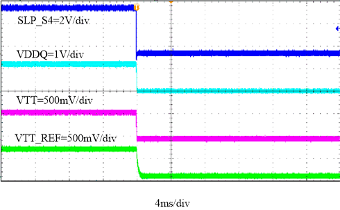
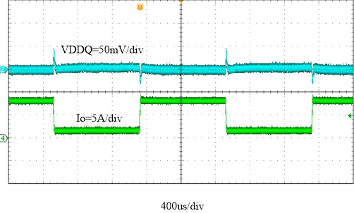
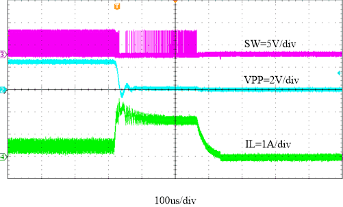
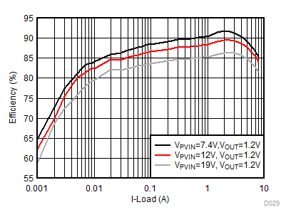
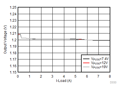
Figure 32 through Figure 60 apply to the circuit of Figure 31. VIN = 12 V. TA = 25°C unless otherwise specified.
TPS65295 D029.gif
Figure 32. VDDQ Efficiency Curve, VOUT = 1.2 V
TPS65295 D030-VDDQloadreg2.gif
Figure 34. VDDQ Load Regulation, VOUT = 1.2 V
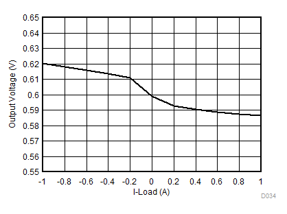
TPS65295 D034-VTTloadreg.gif
Figure 36. VTT Load Regulation, VOUT = 0.6 V
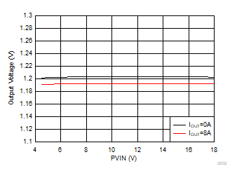
TPS65295 D032-VDDQlinereg.gif
Figure 38. VDDQ Line Regulation,VOUT = 1.2 V
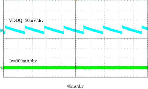
TPS65295 fbd-16-slvsek0.gif
Figure 40. VDDQ Output Voltage Ripple, IOUT = 0 A
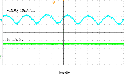
TPS65295 fbd-17-slvsek0.gif
Figure 42. VDDQ Output Voltage Ripple, IOUT = 8 A
TPS65295 fbd-01-slvsek0.gif
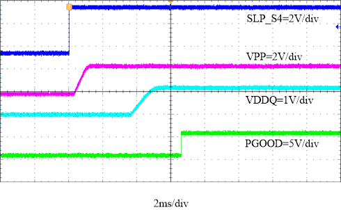
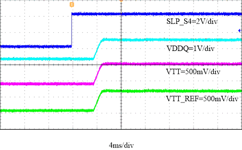
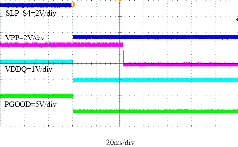
Figure 44. Start-Up Through SLP_S4, IVPPOUT = 0 A, IVDDQOUT = 0 A
TPS65295 fbd-03-slvsek0.gif
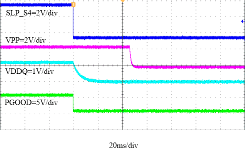
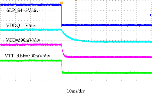
Figure 46. Shutdown Through SLP_S4, IVPPOUT = 0 A, IVDDQOUT = 0 A
TPS65295 fbd-09-slvsek0.gif
IVDDQOUT = 0 A IVTT = 0 A IVTTREF = 0 A
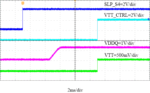
Figure 48. VTT Start-Up Through VTT_CNTL
TPS65295 fbd-11-slvsek0.gif
IVDDQOUT = 0 A IVTT = 0 A IVTTREF = 0 A
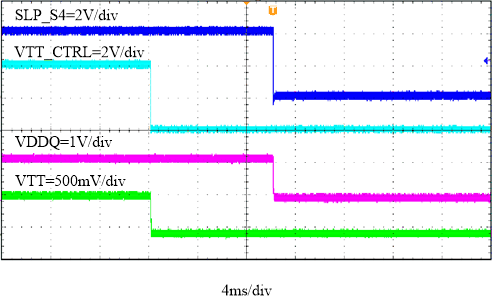
Figure 50. VTT Shutdown Through VTT_CNTL
TPS65295 fbd-05-slvsek0.gif
IVDDQOUT = 0 A IVTT = 0 A IVTTREF = 0 A
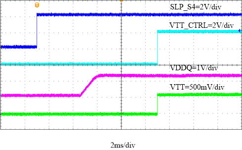
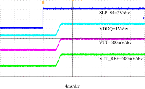
Figure 52. VTT Start-Up Through SLP_S4
TPS65295 fbd-07-slvsek0.gif
IVDDQOUT = 0 A IVTT = 0 A IVTTREF = 0 A
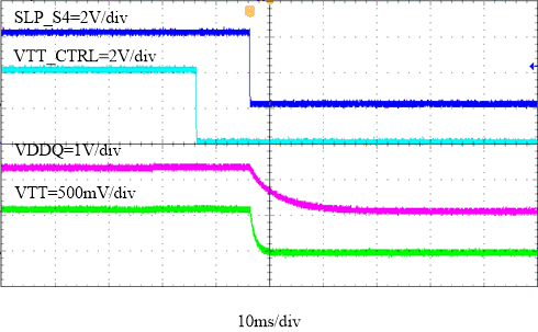
Figure 54. VTT Shutdown Through SLP_S4
TPS65295 fbd-19-slvsek0.gif
Slew Rate=2.5A/us
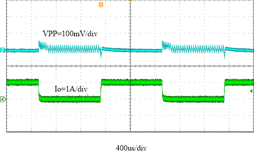
Figure 56. VPP Transient Response, 0 A to 1 A
TPS65295 fbd-14-slvsek0.gif
Slew Rate=2.5A/us
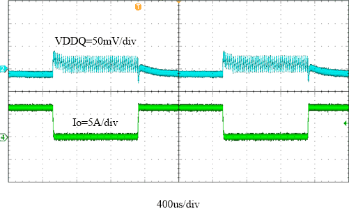
Figure 58. VDDQ Transient Response, 0.1 A to 6.4 A
TPS65295 fbd-13-slvsek0.gif
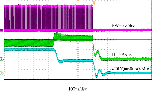
Figure 60. VDDQ Normal Operation to Output Hard Short
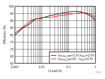
TPS65295 D028-VPPEfficiency.gif
Figure 33. VPP Efficiency Curve, VOUT = 2.5 V
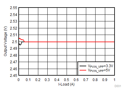
TPS65295 D031-VPPloadregV2.gif
Figure 35. VPP Load Regulation, VOUT = 2.5 V
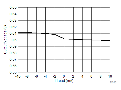
TPS65295 D035-VTTREFloadreg.gif
Figure 37. VTTREF Load Regulation, VOUT = 0.6 V
TPS65295 D033-VPPlineregV2.gif
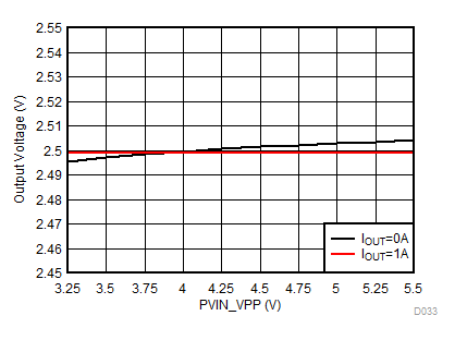
Figure 39. VPP Line Regulation, VOUT = 2.5 V
TPS65295 fbd-20-slvsek0.gif
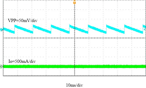
Figure 41. VPP Output Voltage Ripple, IOUT = 0 A
TPS65295 fbd-21-slvsek0.gif
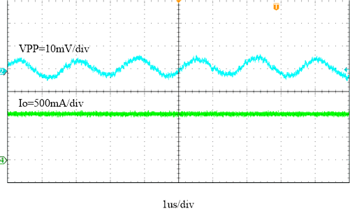
Figure 43. VPP Output Voltage Ripple, IOUT = 1 A
TPS65295 fbd-02-slvsek0.gif
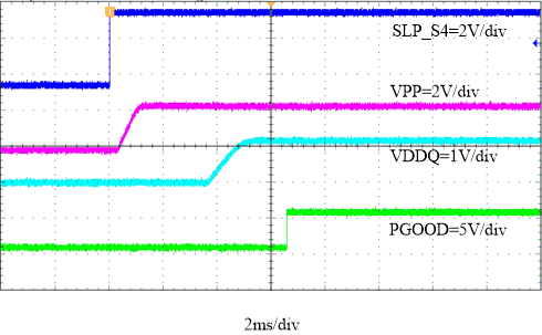
Figure 45. Start-Up Through SLP_S4, IVPPOUT = 1 A, IVDDQOUT = 8 A
TPS65295 fbd-04-slvsek0.gif
Figure 47. Shutdown Through SLP_S4, IVPPOUT = 1 A, IVDDQOUT = 8 A
TPS65295 fbd-10-slvsek0.gif
IVDDQOUT = 8 A IVTT = 1 A IVTTREF = 10m A
Figure 49. VTT Start-Up Through VTT_CNTL
TPS65295 fbd-12-slvsek0.gif
IVDDQOUT = 8 A IVTT = 1 A IVTTREF = 10 mA
Figure 51. VTT Shutdown Through VTT_CNTL
TPS65295 fbd-06-slvsek0.gif
IVDDQOUT = 8 A IVTT = 1 A IVTTREF = 10 mA
Figure 53. VTT Start-Up Through SLP_S4
TPS65295 fbd-08-slvsek0.gif
IVDDQOUT = 8 A IVTT = 1 A IVTTREF = 10 mA
Figure 55. VTT Shutdown Through SLP_S4
TPS65295 fbd-15-slvsek0.gif
Slew Rate=2.5A/us
Figure 57. VDDQ Transient Response, 1.6 A to 8 A
TPS65295 fbd-18-slvsek0.gif
Figure 59. VPP Normal Operation to Output Hard Short