SLVSE55 November 2017 TPS65321A-Q1
PRODUCTION DATA.
- 1 Features
- 2 Applications
- 3 Description
- 4 Revision History
- 5 Pin Configuration and Functions
- 6 Specifications
-
7 Detailed Description
- 7.1 Overview
- 7.2 Functional Block Diagram
- 7.3
Feature Description
- 7.3.1
Buck Regulator
- 7.3.1.1 Fixed-Frequency PWM Control
- 7.3.1.2 Slope Compensation Output
- 7.3.1.3 Pulse-Skip Eco-mode™ Control Scheme
- 7.3.1.4 Dropout Mode Operation and Bootstrap Voltage (BOOT)
- 7.3.1.5 Error Amplifier
- 7.3.1.6 Voltage Reference
- 7.3.1.7 Adjusting the Output Voltage
- 7.3.1.8 Soft-Start Pin (SS)
- 7.3.1.9 Reset Output, nRST
- 7.3.1.10 Overload-Recovery Circuit
- 7.3.1.11 Constant Switching Frequency and Timing Resistor (RT/CLK Pin)
- 7.3.1.12 Overcurrent Protection and Frequency Shift
- 7.3.1.13 Selecting the Switching Frequency
- 7.3.1.14 How to Interface to RT/CLK Pin
- 7.3.1.15 Overvoltage Transient Protection
- 7.3.1.16 Small-Signal Model for Loop Response
- 7.3.1.17 Simple Small-Signal Model for Peak-Current Mode Control
- 7.3.1.18 Small-Signal Model for Frequency Compensation
- 7.3.2 LDO Regulator
- 7.3.3 Thermal Shutdown
- 7.3.4 Enable and Undervoltage Lockout
- 7.3.1
Buck Regulator
- 7.4 Device Functional Modes
-
8 Application and Implementation
- 8.1 Application Information
- 8.2
Typical Application
- 8.2.1
2-MHzSwitching Frequency, 9-V to 16-V Input, 3.3-V Output Buck Regulator, 5-V Output LDO Regulator
- 8.2.1.1 Design Requirements
- 8.2.1.2
Detailed Design Procedure
- 8.2.1.2.1 Switching Frequency Selection for the Buck Regulator
- 8.2.1.2.2 Output Inductor Selection for the Buck Regulator
- 8.2.1.2.3 Output Capacitor Selection for the Buck Regulator
- 8.2.1.2.4 Catch Diode Selection for the Buck Regulator
- 8.2.1.2.5 Input Capacitor Selection for the Buck Regulator
- 8.2.1.2.6 Soft-Start Capacitor Selection for the Buck Regulator
- 8.2.1.2.7 Bootstrap Capacitor Selection for the Buck Regulator
- 8.2.1.2.8 Output Voltage and Feedback Resistor Selection for the Buck Regulator
- 8.2.1.2.9 Frequency Compensation Selection for the Buck Regulator
- 8.2.1.2.10 LDO Regulator
- 8.2.1.2.11 Power Dissipation
- 8.2.1.2.12 Power Dissipation Losses of the LDO Regulator
- 8.2.1.2.13 Total Device Power Dissipation Losses and Junction Temperature
- 8.2.1.3 Application Curves
- 8.2.2 Design Example With 500-kHz Switching Frequency
- 8.2.1
2-MHzSwitching Frequency, 9-V to 16-V Input, 3.3-V Output Buck Regulator, 5-V Output LDO Regulator
- 9 Power Supply Recommendations
- 10Layout
- 11Device and Documentation Support
- 12Mechanical, Packaging, and Orderable Information
Package Options
Mechanical Data (Package|Pins)
- PWP|14
Thermal pad, mechanical data (Package|Pins)
- PWP|14
Orderable Information
6 Specifications
6.1 Absolute Maximum Ratings(1)
over operating free-air temperature (unless otherwise noted)| MIN | MAX | UNIT | |||
|---|---|---|---|---|---|
| Supply inputs | VIN | –0.3 | 40 | V | |
| VIN_LDO | –0.3 | 40 | |||
| Control | EN1, EN2 | –0.3 | 40 | V | |
| EN1-VIN, EN2-VIN | 1 | ||||
| Buck converter | FB1 | –0.3 | 3.6 | V | |
| SW | –0.3 –2 V for 30 ns |
40 | V | ||
| BOOT | –0.3 | 46 | V | ||
| BOOT-SW | 8 | V | |||
| COMP | –0.3 | 3.6 | V | ||
| SS | –0.3 | 3.6 | V | ||
| RT/CLK, SS | –0.3 | 3.6 | V | ||
| nRST | –0.3 | 7 | V | ||
| LDO regulator | LDO_OUT | –0.3 | 7 | V | |
| FB2 | –0.3 | 7 | V | ||
| Operating ambient temperature, TA | -40 | 125 | °C | ||
| Operating junction temperature, TJ | –40 | 150 | °C | ||
| Storage temperature, Tstg | –55 | 165 | °C | ||
(1) Stresses beyond those listed under Absolute Maximum Ratings may cause permanent damage to the device. These are stress ratings only, and functional operation of the device at these or any other conditions beyond those indicated under Recommended Operating Conditions is not implied. Exposure to absolute-maximum-rated conditions for extended periods may affect device reliability.
6.2 ESD Ratings
| VALUE | UNIT | ||||
|---|---|---|---|---|---|
| V(ESD) | Electrostatic discharge | Human-body model (HBM), per AEC Q100-002(1) | ±2000 | V | |
| Charged-device model (CDM), per AEC Q100-011 | All pins | ±500 | |||
| Corner pins (1, 7, 8, and 14) | ±750 | ||||
(1) AEC Q100-002 indicates that HBM stressing shall be in accordance with the ANSI/ESDA/JEDEC JS-001 specification.
6.3 Recommended Operating Conditions
over operating free-air temperature range (unless otherwise noted)| MIN | MAX | UNIT | ||
|---|---|---|---|---|
| Supply inputs | VIN | 3.6 | 36 | V |
| VIN_LDO | 3 | 36 | ||
| Buck regulator | BOOT | 3.6 | 42 | V |
| SW1 | –1 | 36 | ||
| FB1 | 0 | 0.8 | ||
| SS | 0 | 3 | ||
| COMP | 0 | 3 | ||
| RT/CLK | 0 | 3 | ||
| nRST | 0 | 5.25 | ||
| LDO regulator | LDO_OUT | 1.1 | 5.5 | V |
| FB2 | 0 | 0.8 | ||
| Control | EN1 | 0 | 36 | V |
| EN2 | 0 | 36 | ||
| Temperature | Operating junction temperature range, TJ | –40 | 150 | °C |
6.4 Thermal Information
| THERMAL METRIC(1) | TPS65321A-Q1 | UNIT | |
|---|---|---|---|
| PWP (HTSSOP) | |||
| 14 PINS | |||
| RθJA | Junction-to-ambient thermal resistance | 41.0 | °C/W |
| RθJC(top) | Junction-to-case (top) thermal resistance | 33.1 | °C/W |
| RθJB | Junction-to-board thermal resistance | 25.4 | °C/W |
| ψJT | Junction-to-top characterization parameter | 1.6 | °C/W |
| ψJB | Junction-to-board characterization parameter | 25.1 | °C/W |
| RθJC(bot) | Junction-to-case (bottom) thermal resistance | 2.7 | °C/W |
(1) For more information about traditional and new thermal metrics, see the Semiconductor and IC Package Thermal Metrics application report.
6.5 Electrical Characteristics
VI = 6 V to 27 V, EN1 = EN2 = VI, over-operating free-air temperature range TA = –40°C to 125°C and maximum operating junction temperature TJ = –150°C, unless otherwise noted. VI is the voltage on the battery-supply pins, VIN and VIN_LDO.| PARAMETER | TEST CONDITIONS | MIN | TYP | MAX | UNIT | |
|---|---|---|---|---|---|---|
| VIN (INPUT POWER SUPPLY) | ||||||
| Operating input voltage | Normal mode, after initial start-up | 3.6 | 12 | 36 | V | |
| Shutdown supply current | V(EN1) = V(EN2) = 0 V, 25°C | 2 | 7 | μA | ||
| Initial start-up voltage | 6 | 36 | V | |||
| ENABLE AND UVLO (EN1 AND EN2 PINS) | ||||||
| Enable low level | 0.7 | V | ||||
| Enable high level | 2.5 | V | ||||
| V(VIN)(f) | Internal UVLO falling threshold | Ramp V(VIN) down until output turns OFF | 1.8 | 2.6 | 3 | V |
| V(VIN)(r) | Internal UVLO rising threshold | Ramp V(VIN) up until output turns ON | 2.2 | 2.8 | 3.2 | V |
| BUCK REGULATOR | ||||||
| I(Qon) | Operating: non-switching supply | Measured at the VIN pin V(FB1) = 0.83 V, V(VIN) = 12 V, 25°C |
110 | 140 | μA | |
| Output capacitance | ESR = 0.001 Ω to 0.1 Ω, large output capacitance may be required for load transient | 10 | μF | |||
| V(ref1) | Voltage reference for FB1 pin | Buck regulator output: 1.1 V to 20 V. Buck regulator in Continuous Conducting Mode without Pulse-Skipping |
0.788 | 0.8 | 0.812 | V |
| DC output voltage accuracy | Includes voltage references, DC load and line regulation, process and temperature | -2 | 2 | % | ||
| DC(LDR) | DC Load regulation, ΔVOUT / VOUT | IOUT = 0 to IOUTmax | 0.5 | % | ||
| T(LDSR) | Transient load step response | V(VIN) = 12V, IOUT = 200 mA to 3A, TR = TF = 1 µs, Buck Output Voltage = 5V, ƒS = 2 MHz | 5 | % | ||
| BUCK REGULATOR: HIGH-SIDE MOSFET | ||||||
| r(DS(on) HS FET) | On-resistance | V(VIN) = 12 V, V(SW) = 6 V | 127 | 250 | mΩ | |
| tonmin | Minimum on-time | ƒS = 2.5 MHz | 115 | ns | ||
| BUCK REGULATOR: CURRENT-LIMIT | ||||||
| Current-limit threshold | V(VIN) = 12 V, TJ = 25°C | 4 | 6 | A | ||
| BUCK REGULATOR: TIMING RESISTOR AND EXTERNAL CLOCK (RT/CLK PIN) | ||||||
| ƒS | Switching-frequency range | Under RT mode | 100 | 2500 | kHz | |
| Under fixed-frequency PWM mode, with 200 kΩ connected between RT/CLK and GND pins | 523 | 585 | 640 | kHz | ||
| Under CLK mode | 300 | 2200 | kHz | |||
| Minimum CLK input pulse width | Measures at CLK input = 2.2 MHz | 30 | ns | |||
| RT/CLK | High threshold | 1.9 | 2.2 | V | ||
| RT/CLK | Low threshold | 0.5 | 0.7 | V | ||
| RT/CLK | Falling edge to SW rising edge delay | Measured at 500 kHz with external clock connected to RT/CLK pin | 60 | ns | ||
| PLL | Lock-in time | Measured at 500 kHz | 100 | μs | ||
| BUCK REGULATOR: INTERNAL SOFT START TIMER | ||||||
| IDischarge(SS) | Soft-start Pin Discharge Current | V(SS) = 1 V, EN1=0, TA = 25°C | 50 | 400 | μA | |
| V(SS) = 1 V, EN1=0, TA = 125°C | 33 | 400 | μA | |||
| LDO REGULATOR | ||||||
| ΔVO(ΔVI) | Line regulation | V(VIN_LDO) = 6 V to 30 V, I(LDO_OUT) = 10 mA, V(LDO_OUT) = 3.3 V |
20 | mV | ||
| ΔVO(ΔIL) | Load regulation | I(LDO_OUT) = 10 mA to 200 mA, V(VIN_LDO) = 12 V, V(LDO_OUT) = 3.3 V |
35 | mV | ||
| VDROPOUT | Dropout voltage (V(VIN_LDO) – V(LDO_OUT)) |
I(LDO_OUT) = 200 mA | 300 | 450 | mV | |
| I(LDO_OUT) | Output current | V(LDO_OUT) in regulation, V(VIN) ≥ 4V | 280 | mA | ||
| VI(VIN_LDO) | Operating input voltage on VIN_LDO pin | V(LDO_OUT) in regulation | 3 | 36 | V | |
| V(ref2) | Voltage reference at FB2 pin | V(LDO_OUT) = 1.1 V to 5.5 V | 0.788 | 0.8 | 0.812 | V |
| ICL(LDO_OUT) | Output current-limit | V(LDO_OUT) = 0 V (the LDO_OUT pin is shorted to ground) | 280 | 1000 | mA | |
| IQ(LDO) | Quiescent current | V(VIN) = 12 V Measured at VIN pin V(EN1) = 0 V, V(EN2) = 5 V, I(LDO_OUT) = 0.01 mA to 0.75 mA |
35 | 50 | μA | |
| PSRR | Power supply ripple rejection | V(VIN_LDO)(rip) = 0.5 VPP, I(LDO_OUT) = 200 mA, frequency (ƒ) = 100 Hz, V(LDO_OUT) = 5 V and V(LDO_OUT) = 3.3 V |
60 | dB | ||
| V(VIN_LDO)(rip) = 0.5 VPP, I(LDO_OUT) = 200 mA, ƒ = 150 kHz, V(LDO_OUT) = 5 V and V(LDO_OUT) = 3.3 V |
30 | dB | ||||
| C(LDO_OUT) | Output capacitor | ESR = 0.001 Ω to 100 mΩ, large output capacitance may be required for load transient V(LDO_OUT) ≥ 3.3 V |
1 | 40 | μF | |
| C(LDO_OUT) | Output capacitor | ESR = 0.001 Ω to 100 mΩ, large output capacitance may be required for load transient 1.2 V ≤ V(LDO_OUT) < 3.3 V |
20 | 40 | μF | |
| BUCK REGULATOR: RESET (nRST Pin) | ||||||
| RESET threshold | V(FB1) decreasing | 85% | 90% | 95% | ||
| VOL | Output low | nRST pin asserted low due to falling V(FB1), < 1-mA sinking current into nRST pin | 0 | 0.045 | 0.4 | V |
| Filter time | Delay before asserting nRST low | 7 | 14 | 21 | μs | |
| OVER TEMPERATURE PROTECTION | ||||||
| TSD | Thermal-shutdown trip point | 175 | ºC | |||
| Thys | Hysteresis | 10 | ºC | |||
6.6 Typical Characteristics
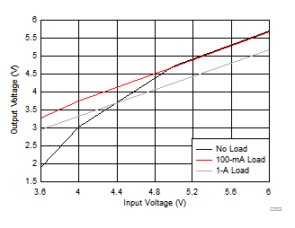
| ƒS = 2 MHz | 3.6 V ≤ V(VIN) ≤ 6 V | |
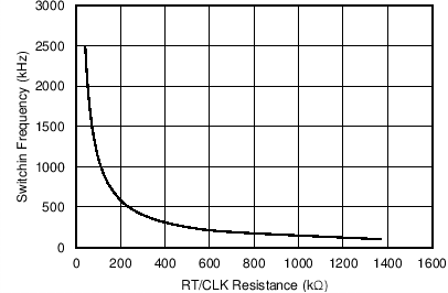
| V(VIN) = 12 V | TJ = 25°C |
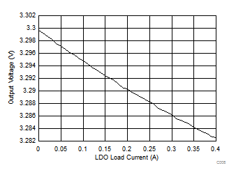
| V(VIN_LDO) = 5 V | V(LDO_OUT) = 3.3 V |
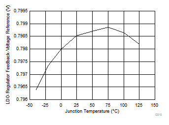
| I(LDO_OUT) = 100 mA | V(VIN_LDO) = 12 V |
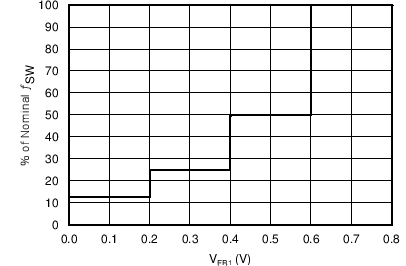
| V(VIN) = 12 V |
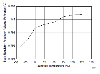
| No Load | V(VIN) = 12 V |
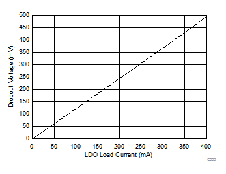
| V(LDO_OUT) = 5 V |