SLVSBK1E September 2012 – May 2014 TPS65631
PRODUCTION DATA.
- 1 Features
- 2 Applications
- 3 Description
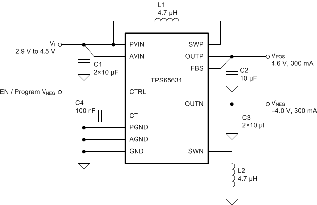
- 4 Simplified Schematic
- 5 Revision History
- 6 Pin Configuration and Functions
- 7 Specifications
-
8 Detailed Description
- 8.1 Overview
- 8.2 Functional Block Diagram
- 8.3 Feature Description
- 8.4 Device Functional Modes
- 9 Applications and Implementation
- 10Power Supply Recommendations
- 11Layout
- 12Device and Documentation Support
- 13Mechanical, Packaging, and Orderable Information
Package Options
Mechanical Data (Package|Pins)
- DPD|12
Thermal pad, mechanical data (Package|Pins)
- DPD|12
Orderable Information
1 Features
- 2.9-V to 4.5-V Input Voltage Range
- Fixed 4.6-V Positive Output Voltage
- 0.5% VPOS Accuracy from 25ºC to 85ºC
- Separate VPOS Output Sense Pin
- Negative Output Voltage Digitally Programmable from –1.4 V to –4.4 V (–4 V Default)
- Output Currents up to 250 mA Supported
- Excellent Line Transient Regulation
- Short-Circuit Protection
- Thermal Shutdown
- Available in 3.00-mm × 3.00-mm, 12-Pin QFN Package
2 Applications
AMOLED Displays
3 Description
The TPS65631 is designed to drive AMOLED (Active Matrix Organic Light Emitting Diode) displays requiring positive and negative supply rails. The device integrates a boost converter for VPOS and an inverting buck boost converter for VNEG and is suitable for battery-operated products. The digital control pin (CTRL) allows programming the negative output voltage in digital steps. The TPS65631 uses a novel technology enabling excellent line transient performance.
- For all available packages, see the orderable addendum at the end of the data sheet