SLVSF06 March 2019 TPS65653-Q1
PRODUCT PREVIEW Information. Product in design phase of development. Subject to change or discontinuance without notice.
- 1 Features
- 2 Applications
- 3 Description
- 4 Revision History
- 5 Pin Configuration and Functions
- 6 Specifications
-
7 Detailed Description
- 7.1 Overview
- 7.2 Functional Block Diagram
- 7.3
Feature Description
- 7.3.1 DC/DC Converters
- 7.3.2 Sync Clock Functionality
- 7.3.3 Power-Up
- 7.3.4 Regulator Control
- 7.3.5 Enable and Disable Sequences
- 7.3.6 Device Reset Scenarios
- 7.3.7 Diagnosis and Protection Features
- 7.3.8 Operation of the GPO Signals
- 7.3.9 Digital Signal Filtering
- 7.4 Device Functional Modes
- 7.5 Programming
- 7.6
Register Maps
- 7.6.1
Register Descriptions
- 7.6.1.1 DEV_REV
- 7.6.1.2 OTP_REV
- 7.6.1.3 BUCK0_CTRL_1
- 7.6.1.4 BUCK0_CTRL_2
- 7.6.1.5 BUCK1_CTRL_1
- 7.6.1.6 BUCK1_CTRL_2
- 7.6.1.7 BUCK0_VOUT
- 7.6.1.8 BUCK1_VOUT
- 7.6.1.9 BUCK0_DELAY
- 7.6.1.10 BUCK1_DELAY
- 7.6.1.11 GPO_DELAY
- 7.6.1.12 GPO2_DELAY
- 7.6.1.13 GPO_CTRL
- 7.6.1.14 CONFIG
- 7.6.1.15 PLL_CTRL
- 7.6.1.16 PGOOD_CTRL_1
- 7.6.1.17 PGOOD_CTRL_2
- 7.6.1.18 PG_FAULT
- 7.6.1.19 RESET
- 7.6.1.20 INT_TOP_1
- 7.6.1.21 INT_TOP_2
- 7.6.1.22 INT_BUCK
- 7.6.1.23 TOP_STAT
- 7.6.1.24 BUCK_STAT
- 7.6.1.25 TOP_MASK_1
- 7.6.1.26 TOP_MASK_2
- 7.6.1.27 BUCK_MASK
- 7.6.1.28 SEL_I_LOAD
- 7.6.1.29 I_LOAD_2
- 7.6.1.30 I_LOAD_1
- 7.6.1
Register Descriptions
- 8 Application and Implementation
- 9 Power Supply Recommendations
- 10Layout
- 11Device and Documentation Support
Package Options
Mechanical Data (Package|Pins)
- RHD|28
Thermal pad, mechanical data (Package|Pins)
- RHD|28
Orderable Information
3 Description
The TPS65653-Q1 is designed to provide a tight power specification for noise sensitive applications, such as radar. The device contains two step-down DC/DC converters and general-purpose digital-output signals. The device is controlled by an I2C-compatible serial interface and by an enable signal.
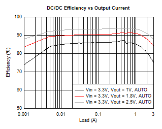
The automatic PWM/PFM (AUTO mode) operation gives high efficiency over a wide output-current range. The TPS65653-Q1 supports remote voltage sensing to compensate IR drop between the regulator output and the point-of-load (POL) thus improving the accuracy of the output voltage. In addition the switching clock can be forced to PWM mode and also synchronized to an external clock to minimize the disturbances.
The TPS65653-Q1 device supports programmable start-up and shutdown delays and sequences including GPO signals synchronized to the enable signal. During start-up and voltage change, the device controls the output slew rate to minimize output voltage overshoot and the in-rush current.
Device Information
| PART NUMBER | PACKAGE | BODY SIZE (NOM) |
|---|---|---|
| TPS65653-Q1 | VQFN (28) | 5.00 mm × 5.00 mm |
- For all available packages, see the orderable addendum at the end of the data sheet.
DC/DC Efficiency vs Output Current
