SLVSAE1B October 2010 – September 2015 TPS65708
PRODUCTION DATA.
- 1 Features
- 2 Applications
- 3 Description
- 4 Revision History
- 5 Pin Configuration and Functions
- 6 Specifications
- 7 Parameter Measurement Information
-
8 Detailed Description
- 8.1 Overview
- 8.2 Functional Block Diagram
- 8.3
Feature Description
- 8.3.1 DC-DC Converters
- 8.3.2 Power Save Mode
- 8.3.3 Dynamic Voltage Positioning
- 8.3.4 Soft Start
- 8.3.5 100% Duty Cycle Low Dropout Operation
- 8.3.6 180° Out-of-Phase Operation
- 8.3.7 Undervoltage Lockout and Enable for DCDC1, DCDC2, LDO1, and LDO2
- 8.3.8 Output Voltage Discharge
- 8.3.9 Power-Up Sequencing
- 8.3.10 Short-Circuit Protection
- 8.3.11 Thermal Shutdown
- 8.3.12 LDOs
- 8.3.13 LED Driver
- 8.4 Device Functional Modes
- 9 Application and Implementation
- 10Power Supply Recommendations
- 11Layout
- 12Device and Documentation Support
- 13Mechanical, Packaging, and Orderable Information
Package Options
Mechanical Data (Package|Pins)
- YZH|16
Thermal pad, mechanical data (Package|Pins)
Orderable Information
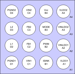
5 Pin Configuration and Functions
YZH Package
16-Pin DSBGA
Bottom View

Pin Functions
| PIN | I/O | DESCRIPTION | |
|---|---|---|---|
| NO. | NAME | ||
| A1 | VLDO1 | O | Output voltage from LDO1 |
| A2 | VINLDO1 | I | Input voltage pin for LDO1 |
| A3 | VINLDO2 | I | Input voltage pin for LDO2 |
| A4 | VLDO2 | O | Output voltage from LDO2 |
| B1 | ISINK | O | Open-drain current sink; connect to the cathode of a LED |
| B2 | PWM | I | Input for LED PWM dimming |
| B3 | MODE | I | Set low to enable Power Save Mode. Pulling this PIN to high forces the device to operate in PWM mode over the whole load range. |
| B4 | VCC | I | Supply Input for internal reference, has to be connected to VIN1 and VIN2 |
| C1 | VIN1 | I | Input voltage pin for buck converter(1) |
| C2 | FB1 | I | Feedback input from buck converter(1) |
| C3 | FB2 | I | Feedback input from buck converter(2) |
| C4 | VIN2 | I | Input voltage pin for buck converter(2) |
| D1 | PGND1 | — | Power ground |
| D2 | L1 | O | Switch output from buck converter(1) |
| D3 | L2 | O | Switch output from buck converter(2) |
| D4 | PGND2 | — | Power ground |
(1) VCC must be the highest input voltage for the device to operate correctly.
(2) VIN1/VIN2 must be connected to VCC.