SWCS049S June   2010  – August 2018 TPS65911

PRODUCTION DATA.  

  1. 1Device Overview
    1. 1.1 Features
    2. 1.2 Applications
    3. 1.3 Description
    4. 1.4 Functional Block Diagram
  2. 2Revision History
  3. 3Device Comparison Table
  4. 4Pin Configuration and Functions
    1. 4.1 Pin Attributes
      1.      Pin Attributes
  5. 5Specifications
    1. 5.1  Absolute Maximum Ratings
    2. 5.2  ESD Ratings
    3. 5.3  Recommended Operating Conditions
    4. 5.4  Thermal Information
    5. 5.5  Electrical Characteristics: I/O Pullup and Pulldown
    6. 5.6  Electrical Characteristics: Digital I/O Voltage
    7. 5.7  Electrical Characteristics: Power Consumption
    8. 5.8  Electrical Characteristics: Power References and Thresholds
    9. 5.9  Electrical Characteristics: Thermal Monitoring and Shutdown
    10. 5.10 Electrical Characteristics: 32-kHz RTC Clock
    11. 5.11 Electrical Characteristics: Backup Battery Charger
    12. 5.12 Electrical Characteristics: VRTC LDO
    13. 5.13 Electrical Characteristics: VIO SMPS
    14. 5.14 Electrical Characteristics: VDD1 SMPS
    15. 5.15 Electrical Characteristics: VDD2 SMPS
    16. 5.16 Electrical Characteristics: VDDCtrl SMPS
    17. 5.17 Electrical Characteristics: LDO1 and LDO2
    18. 5.18 Electrical Characteristics: LDO3 and LDO4
    19. 5.19 Electrical Characteristics: LDO5
    20. 5.20 Electrical Characteristics: LDO6, LDO7, and LDO8
    21. 5.21 Timing and Switching Characteristics
      1. 5.21.1 I2C Timing and Switching
      2. 5.21.2 Switch-ON and Switch-OFF Sequences and Timing
      3. 5.21.3 Power Control Timing
        1. 5.21.3.1 Device State Control Through PWRON Signal
        2. 5.21.3.2 Device SLEEP State Control
        3. 5.21.3.3 Device Turnon and Turnoff With Rising and Falling Input Voltage
        4. 5.21.3.4 Power Supplies State Control Through EN1 and EN2 Signals
        5. 5.21.3.5 VDD1, VDD2 Voltage Control Through EN1 and EN2 Signals
  6. 6Detailed Description
    1. 6.1  Overview
    2. 6.2  Functional Block Diagram
    3. 6.3  Power Reference
    4. 6.4  Power Resources
    5. 6.5  Embedded Power Controller (EPC)
      1. 6.5.1 State Machine
        1. 6.5.1.1 Device POWER ON Enable Conditions
        2. 6.5.1.2 Device POWER ON Disable Conditions
        3. 6.5.1.3 Device SLEEP Enable Conditions
        4. 6.5.1.4 Device Reset Scenarios
      2. 6.5.2 BOOT Configuration, Switch-ON, and Switch-OFF Sequences
      3. 6.5.3 Control Signals
        1. 6.5.3.1  SLEEP
        2. 6.5.3.2  PWRHOLD
        3. 6.5.3.3  BOOT1
        4. 6.5.3.4  NRESPWRON, NRESPWRON2
        5. 6.5.3.5  CLK32KOUT
        6. 6.5.3.6  PWRON
        7. 6.5.3.7  INT1
        8. 6.5.3.8  EN2 and EN1
        9. 6.5.3.9  GPIO0 to GPIO8
        10. 6.5.3.10 HDRST Input
        11. 6.5.3.11 PWRDN
        12. 6.5.3.12 Comparators: COMP1 and COMP2
        13. 6.5.3.13 Watchdog
        14. 6.5.3.14 Tracking LDO
    6. 6.6  PWM and LED Generators
    7. 6.7  Dynamic Voltage Frequency Scaling and Adaptive Voltage Scaling Operation
    8. 6.8  32-kHz RTC Clock
    9. 6.9  Real Time Clock (RTC)
      1. 6.9.1 Time Calendar Registers
      2. 6.9.2 General Registers
      3. 6.9.3 Compensation Registers
    10. 6.10 Backup Battery Management
    11. 6.11 Backup Registers
    12. 6.12 I2C Interface
      1. 6.12.1 Access Protocols
        1. 6.12.1.1 Single Byte Access
        2. 6.12.1.2 Multiple Byte Access to Several Adjacent Registers
    13. 6.13 Thermal Monitoring and Shutdown
    14. 6.14 Interrupts
    15. 6.15 Register Maps
      1. 6.15.1 Functional Registers
        1. 6.15.1.1 TPS65911_FUNC_REG Registers Mapping Summary
        2. 6.15.1.2 TPS65911_FUNC_REG Register Descriptions
  7. 7Applications, Implementation, and Layout
    1. 7.1 Application Information
    2. 7.2 Typical Application
      1. 7.2.1 Design Requirements
      2. 7.2.2 Detailed Design Procedure
        1. 7.2.2.1 External Component Recommendation
        2. 7.2.2.2 Controller Design Procedure
          1. 7.2.2.2.1 Inductor Selection
          2. 7.2.2.2.2 Selecting the RTRIP Resistor
          3. 7.2.2.2.3 Selecting the Output Capacitors
          4. 7.2.2.2.4 Selecting FETs
          5. 7.2.2.2.5 Bootstrap Capacitor
          6. 7.2.2.2.6 Selecting Input Capacitors
        3. 7.2.2.3 Converter Design Procedure
          1. 7.2.2.3.1 Selecting the Inductor
          2. 7.2.2.3.2 Selecting Output Capacitors
          3. 7.2.2.3.3 Selecting Input Capacitors
      3. 7.2.3 Application Curves
      4. 7.2.4 Layout Guidelines
        1. 7.2.4.1 PCB Layout
      5. 7.2.5 Layout Example
    3. 7.3 Power Supply Recommendations
  8. 8Device and Documentation Support
    1. 8.1 Device Support
      1. 8.1.1 Development Support
      2. 8.1.2 Device Nomenclature
    2. 8.2 Documentation Support
      1. 8.2.1 Related Documentation
    3. 8.3 Receiving Notification of Documentation Updates
    4. 8.4 Community Resources
      1. 8.4.1 Community Resources
    5. 8.5 Trademarks
    6. 8.6 Electrostatic Discharge Caution
    7. 8.7 Glossary
  9. 9Mechanical, Packaging, and Orderable Information
    1. 9.1 Package Description

Package Options

Mechanical Data (Package|Pins)
Thermal pad, mechanical data (Package|Pins)
Orderable Information

State Machine

The EPC supports the following states:

  • NO SUPPLY: The primary battery supply voltage is not high enough to power the VRTC regulator. A global reset is asserted in this case. Everything on the device is off.
  • BACKUP: The primary battery supply voltage is high enough to enable the VRTC domain but not enough to switch on all the resources. In this state, the VRTC regulator is in backup mode and only the 32K oscillator and RTC module are operating (if enabled). All other resources are off or under reset.
  • OFF: The primary battery supply voltage is high enough to start the power-up sequence, but device power on is not enabled. All power supplies are in the OFF state except VRTC.
  • ACTIVE: Device POWER ON enable conditions are met and regulated power supplies are on or can be enabled with full current capability.
  • SLEEP: Device SLEEP enable conditions are met and some selected regulated power supplies are in low-power mode.

Figure 6-1 shows the transitions for the state machine.
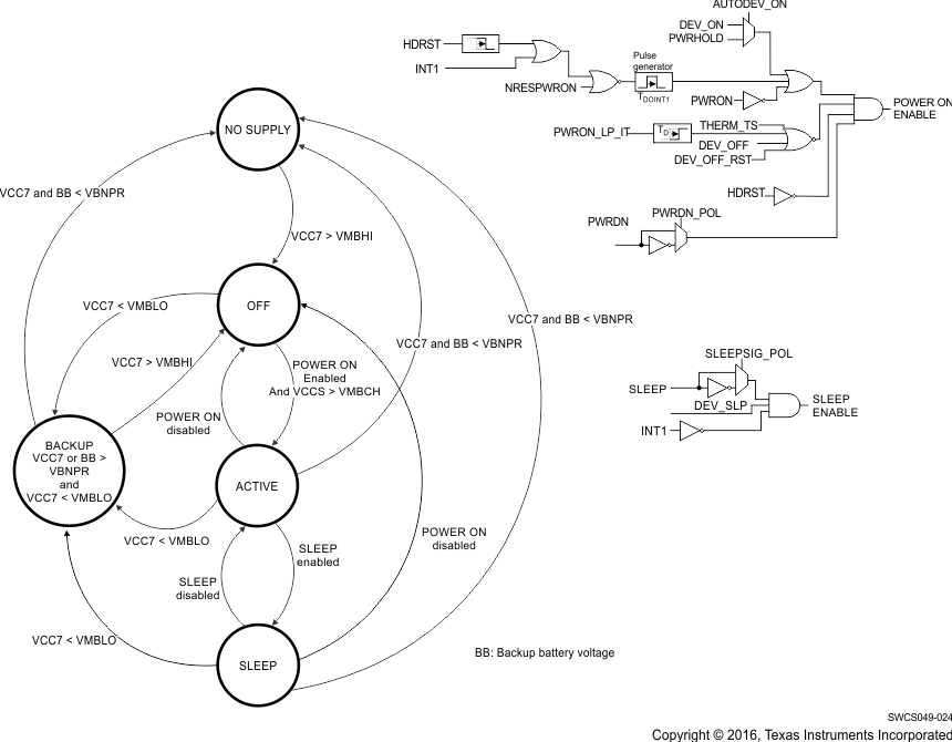
TPS65911 SWCS049-024.gif

NOTE:

PWRHOLD enables power-on unless the pin is programmed as GPI.
Figure 6-1 Embedded Power Control State Machine