SWCS071C August 2012 – August 2017
PRODUCTION DATA.
- 1 Device Overview
- 2 Revision History
- 3 Default Settings
- 4 Pin Configuration and Functions
-
5 Specifications
- 5.1 Absolute Maximum Ratings
- 5.2 ESD Ratings
- 5.3 Recommended Operating Conditions
- 5.4 Thermal Characteristics
- 5.5 Electrical Characteristics - DCDC1, DCDC2, and DCDC3
- 5.6 Electrical Characteristics - DCDC4
- 5.7 Electrical Characteristics - LDOs
- 5.8 Electrical Characteristics - Digital Inputs, Digital Outputs
- 5.9 Electrical Characteristics - VMON Voltage Monitor, VDDIO, Undervoltage Lockout (UVLO), and LDOAO
- 5.10 Electrical Characteristics - Load Switch
- 5.11 Electrical Characteristics - LED Drivers
- 5.12 Electrical Characteristics - Thermal Monitoring and Shutdown
- 5.13 Electrical Characteristics - 32-kHz RC Clock
- 5.14 SPI Interface Timing Requirements
- 5.15 I2C Interface Timing Requirements
- 5.16 Typical Characteristics
- 6 Parameter Measurement Information
-
7 Detailed Description
- 7.1 Overview
- 7.2 Functional Block Diagram
- 7.3 Linear Regulators
- 7.4 Step-Down Converters
- 7.5 GPIOs
- 7.6 Power State Machine
- 7.7 Transition Conditions
- 7.8 Implementation of Internal Power-Up and Power-Down Sequencing
- 7.9 EN1, EN2, EN3, EN4, Resources Control
- 7.10 SLEEP State Control
- 7.11 Registers SET_OFF, KEEP_ON and DEF_VOLT Used in SLEEP State; CONFIG2 = 1
- 7.12 Registers SET_OFF, KEEP_ON and DEF_VOLT Used for Resources Assigned to an External Enable Pin; CONFIG2 = 1
- 7.13 Registers SET_OFF, KEEP_ON and DEF_VOLT for Resources Assigned to Pins PWR_REQ, CLK_REQ1 and CLK_REQ2; CONFIG2 = 0
- 7.14 Voltage Scaling Interface Control Using _OP and _AVS Registers with I2C or SPI Interface
- 7.15 Voltage Scaling Using the VCON Decoder on Pins VCON_PWM and VCON_CLK
- 7.16 Configuration Pins CONFIG1, CONFIG2 and DEF_SPI_I2C-GPIO
- 7.17 VDDIO Voltage for Push-Pull Output Stages
- 7.18 Digital Signal Summary
- 7.19 TPS659121 On/Off Operation With E450, E500
- 7.20 TPS659122 On/Off Operation for CONFIG1=HIGH
- 7.21 TPS659122 On/Off Operation for CONFIG1=LOW
- 7.22 Interfaces
- 7.23 Serial Peripheral Interface
- 7.24 I2C Interface
- 7.25 Thermal Monitoring and Shutdown
- 7.26 Load Switch
- 7.27 LED Driver
- 7.28
Memory
- 7.28.1 Register Format
- 7.28.2
Register Descriptions
- 7.28.2.1
DCDC Registers
- 7.28.2.1.1 DCDC1_CTRL (00h)
- 7.28.2.1.2 DCDC2_CTRL (01h)
- 7.28.2.1.3 DCDC3_CTRL (02h)
- 7.28.2.1.4 DCDC4_CTRL (03h)
- 7.28.2.1.5 DCDC1_OP (04h)
- 7.28.2.1.6 DCDC1_AVS (05h)
- 7.28.2.1.7 DCDC1_LIMIT (06h)
- 7.28.2.1.8 DCDC2_OP (07h)
- 7.28.2.1.9 DCDC2_AVS (08h)
- 7.28.2.1.10 DCDC2_LIMIT (09h)
- 7.28.2.1.11 DCDC3_OP (0Ah)
- 7.28.2.1.12 DCDC3_AVS (0Bh)
- 7.28.2.1.13 DCDC3_LIMIT (0Ch)
- 7.28.2.1.14 DCDC4_OP (0Dh)
- 7.28.2.1.15 DCDC4_AVS (0Eh)
- 7.28.2.1.16 DCDC4_LIMIT (0Fh)
- 7.28.2.1.17 VDCDCx Range Settings
- 7.28.2.1.18 DCDCx Voltage Settings
- 7.28.2.2
LDO Registers
- 7.28.2.2.1 LDO1_OP (10h)
- 7.28.2.2.2 LDO1_AVS (11h)
- 7.28.2.2.3 LDO1_LIMIT (12h)
- 7.28.2.2.4 LDO2_OP (13h)
- 7.28.2.2.5 LDO2_AVS (14h)
- 7.28.2.2.6 LDO2_LIMIT (15h)
- 7.28.2.2.7 LDO3_OP (16h)
- 7.28.2.2.8 LDO3_AVS (17h)
- 7.28.2.2.9 LDO3_LIMIT (18h)
- 7.28.2.2.10 LDO4_OP (19h)
- 7.28.2.2.11 LDO4_AVS (1Ah)
- 7.28.2.2.12 LDO4_LIMIT (1Bh)
- 7.28.2.2.13 LDO5 (1Ch)
- 7.28.2.2.14 LDO6 (1Dh)
- 7.28.2.2.15 LDO7 (1Eh)
- 7.28.2.2.16 LDO8 (1Fh)
- 7.28.2.2.17 LDO9 (20h)
- 7.28.2.2.18 LDO10 (21h)
- 7.28.2.3 LDO Voltage Settings
- 7.28.2.4
DEVCTRL Registers
- 7.28.2.4.1 THRM_REG (22h)
- 7.28.2.4.2 CLK32KOUT (23h)
- 7.28.2.4.3 DEVCTRL (24h)
- 7.28.2.4.4 DEVCTRL2 (25h)
- 7.28.2.4.5 I2C_SPI_CFG (26h)
- 7.28.2.4.6 KEEP_ON1 (27h)
- 7.28.2.4.7 KEEP_ON2 (28h)
- 7.28.2.4.8 SET_OFF1 (29h)
- 7.28.2.4.9 SET_OFF2 (2Ah)
- 7.28.2.4.10 DEF_VOLT (2Bh)
- 7.28.2.4.11 LDO Sleep Mode Behavior
- 7.28.2.4.12 DEF_VOLT_MAPPING (2Ch)
- 7.28.2.4.13 DISCHARGE1 (2Dh)
- 7.28.2.4.14 DISCHARGE2 (2Eh)
- 7.28.2.4.15 EN1_SET1 (2Fh)
- 7.28.2.4.16 EN1_SET2 (30h)
- 7.28.2.4.17 EN2_SET1 (31h)
- 7.28.2.4.18 EN2_SET2 (32h)
- 7.28.2.4.19 EN3_SET1 (33h)
- 7.28.2.4.20 EN3_SET2 (34h)
- 7.28.2.4.21 EN4_SET1 (35h)
- 7.28.2.4.22 EN4_SET2 (36h)
- 7.28.2.4.23 PGOOD (37h)
- 7.28.2.4.24 PGOOD2 (38h)
- 7.28.2.4.25 INT_STS (39h)
- 7.28.2.4.26 INT_MSK (3Ah)
- 7.28.2.4.27 INT_STS2 (3Bh)
- 7.28.2.4.28 INT_MSK2 (3Ch)
- 7.28.2.4.29 INT_STS3 (3Dh)
- 7.28.2.4.30 INT_MSK3 (3Eh)
- 7.28.2.4.31 INT_STS4 (3Fh)
- 7.28.2.4.32 INT_MSK4 (40h)
- 7.28.2.4.33 GPIO1 (41h)
- 7.28.2.4.34 GPIO2 (42h)
- 7.28.2.4.35 GPIO3 (43h)
- 7.28.2.4.36 GPIO4 (44h)
- 7.28.2.4.37 GPIO5 (45h)
- 7.28.2.4.38 VMON (46h)
- 7.28.2.4.39 LEDA_CTRL1 (47h)
- 7.28.2.4.40 LEDA_CTRL2 (48h)
- 7.28.2.4.41 LEDA_CTRL3 (49h)
- 7.28.2.4.42 LEDA_CTRL4 (4Ah)
- 7.28.2.4.43 LEDA_CTRL5 (4Bh)
- 7.28.2.4.44 LEDA_CTRL6 (4Ch)
- 7.28.2.4.45 LEDA_CTRL7 (4Dh)
- 7.28.2.4.46 LEDA_CTRL8 (4Eh)
- 7.28.2.4.47 LEDB_CTRL1 (4Fh)
- 7.28.2.4.48 LEDB_CTRL2 (50h)
- 7.28.2.4.49 LEDB_CTRL3 (51h)
- 7.28.2.4.50 LEDB_CTRL4 (52h)
- 7.28.2.4.51 LEDB_CTRL5 (53h)
- 7.28.2.4.52 LEDB_CTRL6 (54h)
- 7.28.2.4.53 LEDB_CTRL7 (55h)
- 7.28.2.4.54 LEDB_CTRL8 (56h)
- 7.28.2.4.55 LEDC_CTRL1 (57h)
- 7.28.2.4.56 LEDC_CTRL2 (58h)
- 7.28.2.4.57 LEDC_CTRL3 (59h)
- 7.28.2.4.58 LED_CTRL4 (5Ah)
- 7.28.2.4.59 LEDC_CTRL5 (5Bh)
- 7.28.2.4.60 LEDC_CTRL6 (5Ch)
- 7.28.2.4.61 LEDC_CTRL7 (5Dh)
- 7.28.2.4.62 LEDC_CTRL8 (5Eh)
- 7.28.2.4.63 LED_RAMP_UP_TIME (5Fh)
- 7.28.2.4.64 LED_RAMP_DOWN_TIME (60h)
- 7.28.2.4.65 LED_SEQ_EN (61h)
- 7.28.2.4.66 LEDx DC Current
- 7.28.2.4.67 LOADSWITCH (62h)
- 7.28.2.4.68 SPARE (63h)
- 7.28.2.4.69 VERNUM (64h)
- 7.28.2.1
DCDC Registers
- 8 Applications, Implementation, and Layout
- 9 Device and Documentation Support
- 10Mechanical, Packaging, and Orderable Information
Package Options
Mechanical Data (Package|Pins)
- YFF|81
Thermal pad, mechanical data (Package|Pins)
Orderable Information
5 Specifications
5.1 Absolute Maximum Ratings
over operating free-air temperature range (unless otherwise noted)(1)| MIN | MAX | UNIT | ||
|---|---|---|---|---|
| Voltage | All pins except A/PGND pins and pins listed below with respect to AGND | –0.3 | 6 | V |
| VLDO1, VLDO2, VLDO3, VLDO4, VLDO5, VLDO6, VLDO7,VLDO8, VLDO9, VLDO10, VINLDO1210, VINLDO3, EN1 (DCDC1_SEL), EN2 (DCDC2_SEL), EN3 (DCDC3_SEL), EN4 (DCDC4_SEL) SLEEP (PWR_REQ), CLK_REQ1, CLK_REQ2 VDDIO, CONFIG1, CONFIG2, DEF_SPI_I2C-GPIO, EN_LS0, EN_LS1, OMAP_WDI, CPCAP_WDI, VCON_CLK with respect to AGND |
–0.3 | 3.6 | ||
| Pin VDCDC1, VDCDC2, VDCDC3, VDCDC4 with respect to AGND | –0.3 | 3.8 | ||
| Pins SDA_SDI, SCL_SCK, SDO_GPIO1, SCE_GPIO2, SDA_AVS, SCL_AVS, INT1, 32KCLKOUT,GPIO3 and GPIO4 and GPIO5 if defined as GPIOs with push-pull output (otherwise it is 6-V rated), NRESPWRON if nRESPWRON is push-pull output (otherwise it is 6-V rated) with respect to AGND | –0.3 | VDDIO + 0.3 | ||
| VCC | VDDIO | 6 | ||
| Current | All non power pins | 5 | mA | |
| Power pins (per pin) | 2 | A | ||
| Operating free-air temperature, TA | –40 | 85 | °C | |
| Maximum junction temperature, TJ | 125 | °C | ||
| Storage temperature range, Tstg | –65 | 150 | °C | |
(1) Stresses beyond those listed under Absolute Maximum Ratings may cause permanent damage to the device. These are stress ratings only and functional operation of the device at these or any other conditions beyond those indicated under Section 5.3 is not implied. Exposure to absolute-maximum-rated conditions for extended periods may affect device reliability.
5.2 ESD Ratings
| VALUE | UNIT | |||
|---|---|---|---|---|
| VESD | Electrostatic discharge | Human body model (HBM), per ANSI/ESDA/JEDEC JS001(1) | 1000 | V |
| Charged device model (CDM), per JESD22-C101(2) | 250 | V | ||
(1) JEDEC document JEP155 states that 500-V HBM allows safe manufacturing with a standard ESD control process.
(2) JEDEC document JEP157 states that 250-V CDM allows safe manufacturing with a standard ESD control process.
5.3 Recommended Operating Conditions
over operating free-air temperature range (unless otherwise noted)| MIN | NOM | MAX | UNIT | ||
|---|---|---|---|---|---|
| DC-DC CONVERTERS | |||||
| VIN1, VIN2, VIN3, VIN4 | Input voltage for step-down converter DCDC1, DCDC2, DCDC3, DCDC4 | 2.7 | 5.5 | V | |
| Output voltage for step-down converter DCDC1, DCDC2, DCDC3(1) | 0.5 | 3.8 | V | ||
| Output voltage for step-down converter DCDC4(1) | 0.5 | 3.8 | V | ||
| Inductance at L2, L3 | 0.5 | 1.0 | 1.3 | μH | |
| Inductance at L1, L4 | 0.5 | 1.0 | 1.3 | μH | |
| CIN1 , CIN4 | Input capacitance at VIN1 and VIN4 (on each pin) | 10 | 22 | μF | |
| CIN2 , CIN3 | Input capacitance at VIN2 and VIN3 (on each pin) | 4.7 | 10 | μF | |
| COUTDCDC1,2,3 | Output capacitance at DCDC1, DCDC2 and DCDC3 | 4.7 | 10 | 22 | μF |
| COUTDCDC4 | Output capacitance at DCDC4 | 10 | 22 | 47 | μF |
| LDOs | |||||
| VINLDO1210 | Input voltage range for LDO1, LDO2 and LDO10 | 1.7 | 3.6 | V | |
| VINLDO4 | Input voltage range for LDO4 | 1.9 | 5.5 | V | |
| VINLDO5 | Input voltage range for LDO5 | 1.9 | 5.5 | V | |
| VLDO1, VLDO2,
VLDO3, VLDO6, VLDO7, VLDO8, VLDO9, VLDO10 |
Output voltagefor general purpose (GP) LDOs(1) | 0.8 | 3.3 | V | |
| VLDO4, VLDO5, | Output voltage for RF-LDOs | 1.6 | 3.3 | V | |
| CINLDO1210
CINLDO3, CINLDO4, CINLDO5, CINLDO67 CINLDO8 CINLDO8 |
Input capacitance on LDO supply pins | 0.5 | μF | ||
| CoutLDO4,
CoutLDO5 |
Output capacitance on LDO4 and LDO5 | 2.2 | 10 | μF | |
| CoutLDO1,
CoutLDO2 CoutLDO3 CoutLDO6 CoutLDO7 CoutLDO8 |
Output capacitance LDO1, LDO2, LDO3, LDO6, LDO7, LDO8 These LDOs are capless, the required capacitance can be placed at the load |
0.5 | 10 | μF | |
| CoutLDO9
CoutLDO10 |
Output capacitance LDO9 and LDO10 These LDOs are capless, the required capacitance can be placed at the load |
1 | 10 | μF | |
| CoutLDOAO | Output capacitance on LDOAO | 0.5 | 10 | μF | |
| CVIN_DCDC_ANA | Input capacitance on VIN_DCDC_ANA | 100 | nF | ||
| CVCC | Input capacitance on VCC | 100 | nF | ||
| CVDDIO | Input capacitance on VDDIO | 100 | nF | ||
| TA | Operating ambient temperature | –40 | 85 | °C | |
| TJ | Operating junction temperature | –40 | 125 | °C | |
(1) The maximum output voltage of DCDC1 to DCDC4 and LDO1 to LDO4 can be reduced by a OTP setting to adopt the maximum voltage to the requirements (or maximum ratings) of the load powered. This allows to protect the processor from exceeding the maximum ratings for the core voltage. The value is set at TI upon customer request in nonvolatile memory (OTP).
5.4 Thermal Characteristics
| THERMAL METRIC(1) | TPS65912 | UNIT | |
|---|---|---|---|
| YFF (DSBGA) | |||
| 81 PINS | |||
| RθJA | Junction-to-ambient thermal resistance | 41.3 | °C/W |
| RθJCtop | Junction-to-case (top) thermal resistance | 0.1 | °C/W |
| RθJB | Junction-to-board thermal resistance | 5.2 | °C/W |
| ψJT | Junction-to-top characterization parameter | 0.7 | °C/W |
| ψJB | Junction-to-board characterization parameter | 5.2 | °C/W |
(1) For more information about traditional and new thermal metrics, see Semiconductor and IC Package Thermal Metrics.
5.5 Electrical Characteristics – DCDC1, DCDC2, and DCDC3
TA = –40°C to +85°C, typical values are at TA = +25°C (unless otherwise noted)| PARAMETER | TEST CONDITION | MIN | TYP | MAX | UNIT | |
|---|---|---|---|---|---|---|
| VIN | Input Voltage Range | 2.3 | 5.5 | V | ||
| VDCDC1
VDCDC2 VDCDC3 |
DCDCx Output Voltage Range | Option1; in 12.5-mV steps; RANGE[1,0] = 00 | 0.5 | 1.2875 | V | |
| Option2; in 12.5-mV steps; RANGE[1,0] = 01 | 0.7 | 1.4875 | V | |||
| Option3; in 25-mV steps; RANGE[1,0] = 10 | 0.5 | 2.075 | V | |||
| Option4; in 50-mV steps; RANGE[1,0] = 11 | 0.5 | 3.80 | V | |||
| IOUT(DCDCx) | Continuous Output Current | DCDC1 (VINDCDC1 ≥ 2.8 V) | 2500 | mA | ||
| DCDC2 (VINDCDC2 ≥ 2.8 V) | 750 | |||||
| DCDC3 (VINDCDC3 ≥ 2.8 V) | 1200 | |||||
| DCDC3 for VIN= 2.8 V to 4.5 V; VDCDC3(max) = 1.4875 V |
1600 | |||||
| IQ | Quiescent Current | ILOAD = 0 mA, DCDCx_MODE = 0, Device not switching; for DCDC1 | 26 | 55 | μA | |
| ILOAD = 0 mA, DCDCx_MODE = 1, Device switching; for DCDC1 |
8 | mA | ||||
| ILOAD < 1 mA, Device not switching; ECO = 1 AND DCDCx_MODE = 0, for DCDC1 | 9 | μA | ||||
| ILOAD = 0 mA, DCDCx_MODE = 0, Device not switching, for DCDC2 or DCDC3 | 26 | 40 | μA | |||
| ILOAD = 0 mA, DCDCx_MODE = 1, Device switching, for DCDC2 or DCDC3 |
8 | mA | ||||
| ILOAD < 1 mA, Device not switching; ECO = 1 AND DCDCx_MODE = 0, for DCDC2 or DCDC3 | 3 | μA | ||||
| VDCDC1/2/3 | Accuracy | DCDCx_MODE = 1, VIN = 3.6 V, ILOAD = 0 mA, TA = 25°C, ECO = 0 | –2% | |||
| DCDCx_MODE = 1, VIN = 3.6 V, ILOAD = 0 mA, TA = –40°C – 85°C, ECO = 0 |
–2.5% | |||||
| DCDCx_MODE = 0, VIN = 3.6 V, ILOAD = 0 mA, TA = 25°C, ECO = 0 | –3% | |||||
| ECO Mode Accuracy | VIN = 3.6 V, ILOAD = 0 mA, TA = –40 – 85°C; ECO = 1 AND DCDCx_MODE = 0 | –5% | 5% | |||
| Load Regulation | DCDCx_MODE = 1, VIN = 3.6 V; ILOAD = 120 mA to 1080 mA; for DCDC1 |
0.01 | %/A | |||
| DCDCx_MODE = 1, VIN = 3.6 V; ILOAD = 120 mA to 1080 mA; for DCDC3 |
0.01 | |||||
| DCDCx_MODE = 1, VIN = 3.6 V; ILOAD = 50 mA to 450 mA; for DCDC2 |
0.01 | |||||
| Line Regulation | DCDCx_MODE = 1, VIN = 2.5 to 5.5 V, ILOAD = 0 mA, for DCDC1 |
0.01 | %/V | |||
| DCDCx_MODE = 1, VIN = 2.5 to 5.5 V, ILOAD = 0 mA, for DCDC2 or DCDC3 |
0.01 | |||||
| fSW | Switching Frequency | DCDCx_MODE = 0 | 3500 | kHz | ||
| DCDCx_MODE = 1, VIN = 3.6 V, VOUT = 1.8 V | 2800 | kHz | ||||
| RDS(ON) | High-Side FET On-Resistance | for DCDC1 with VIN_DCDCx = 3.6 V, D = 100% |
60 | 100 | mΩ | |
| for DCDC2 and DCDC3 with VIN_DCDCx = 3.6 V, D = 100% |
120 | 190 | mΩ | |||
| RDS(ON) | Low-Side FET On-Resistance | for DCDC1 with VIN_DCDCx = 3.6 V, D = 100% | 60 | 100 | mΩ | |
| for DCDC2 and DCDC3 with VIN_DCDCx = 3.6 V, D = 100% |
100 | 160 | mΩ | |||
| ILK_HS | High-Side FET Leakage Current | TJ = 85°C; DCDC1; VINDCDC1 = 4.2 V | 20 | μA | ||
| TJ = 85°C; DCDC2 or DCDC3; VINDCDC2 = VINDCDC3 = 4.2 V |
3 | |||||
| ILK_LS | Low-Side FET Leakage Current | TJ = 85°C; DCDC1; VINDCDC1 = 4.2 V | 20 | μA | ||
| TJ = 85°C; DCDC2 or DCDC3; VINDCDC2 = VINDCDC3 = 4.2 V |
1 | |||||
| IHS_LIMF | High-Side Forward Current Limit | VIN = 3.6 V; DCDC1 | 3200 | 4280 | 5300 | mA |
| VIN = 3.6 V; DCDC2 | 1250 | 1667 | 2083 | |||
| VIN = 3.6 V; DCDC3 | 2100 | 2800 | 3500 | |||
| ILS_LIMF | Low-Side Forward Current Limit | VIN = 3.6 V; DCDC1 | 3200 | 4280 | 5300 | mA |
| VIN = 3.6 V; DCDC2 | 1200 | 1600 | 2000 | |||
| VIN = 3.6 V; DCDC3 | 1875 | 2500 | 3125 | |||
| tOFF(MIN) | Minimum HS FET Off Time | VIN = 3.6 V | 30 | ns | ||
| DCDC1 output voltage ripple | VIN = 5 V; VOUT = 0.95 V; Io = 1.5 A; L = 1 µH, RSL = 50 mR; Co = 10 µF |
10 | mVpp | |||
| DCDC2 output voltage ripple | VIN = 5 V; VOUT = 2.0 V; Io = 600 mA; L = 1 µH, RSL = 50 mR; Co = 10 µF |
10 | mVpp | |||
| DCDC3 output voltage ripple | VIN = 5 V; VOUT = 3.2 V; Io = 600 mA; L = 1 µH, RSL = 50 mR; Co = 10 µF |
10 | mVpp | |||
| DCDC1 load transient response | VIN = 5 V; VOUT = 0.95 V; Io = 1 mA to 2 A; L = 1 µH, RSL = 50 mR; Co = 10 µF; dt = 100 ns |
25 | mV | |||
| DCDC2 load transient response | VIN = 5 V; VOUT = 1.8 V; Io = 1 mA to 400 mA; L = 1 µH, RSL = 50 mR; Co = 10 µF; dt = 1 µs |
50 | mV | |||
| DCDC3 load transient response | VIN = 5 V; VOUT = 3.2 V; Io = 1 mA to 500 mA; L = 1 µH, RSL = 50 mR; Co = 10 µF; dt = 1 µs |
50 | mV | |||
| VDCDCPG | Power Good Threshold | VDCDCx falling | 86% | 90% | 94% | |
| VDCDCx rising | 98% | |||||
| tDCDCPG | Power Good Threshold Deglitch | 1 | ms | |||
| tStart | Start-up time | Time to start switching, measured from end of I2C command enabling converter | 32 | 55 | 100 | μs |
| tRamp | VOUT Ramp UP time | Time to ramp from 5% to 95% of VOUT | 100 | 160 | 250 | μs |
| RDischarge | Discharge resistor | 250 | 400 | 500 | Ω | |
| Tpwm | PWM clock period for VCON_CLK | 30 | 300 | ns | ||
| Tsu | VCON set up time | VCON_PWM to rising edge of VCON_CLK | 7 | ns | ||
| Thd | VCON hold time | VCON_PWM from rising edge of VCON_CLK | 7 | ns | ||
5.6 Electrical Characteristics – DCDC4
TA = –40°C to +85°C, typical values are at TA = +25°C (unless otherwise noted)| PARAMETER | TEST CONDITIONS | MIN | TYP | MAX | UNIT | |
|---|---|---|---|---|---|---|
| VIN | Input Voltage Range | 2.3 | 5.5 | V | ||
| VDCDC4 | DCDC4 Output Voltage Range | Option1; in 12.5-mV steps; RANGE[1,0] = 00 | 0.5 | 1.2875 | V | |
| Option2; in 12.5-mV steps; RANGE[1,0] = 01 | 0.7 | 1.4875 | ||||
| Option3; in 25-mV steps; RANGE[1,0] = 10 | 0.5 | 2.075 | ||||
| Option4; in 50-mV steps; RANGE[1,0] = 11 | 0.5 | 3.80 | ||||
| IOUT(DCDC4) | Continuous Output Current | DCDC4 (VINDCDC4 ≥ 2.8 V) | 2500 | mA | ||
| IQ | Quiescent Current | ILOAD = 0 mA, DCDC4_MODE = 0, Device not switching | 26 | 55 | μA | |
| ILOAD = 0 mA, DCDC4_MODE = 1, Device switching; EN_LS[1,0] = 00 or 01 | 8 | mA | ||||
| ILOAD < 1 mA, Device not switching; ECO = 1 AND DCDC4_MODE = 0 | 9 | μA | ||||
| VDCDCx | Accuracy | DCDC4_MODE = 1, VIN = 3.6 V, ILOAD = 0 mA, TA = 25°C; EN_LS[1,0] = 00 or 01 |
–2% | 2% | ||
| DCDC4_MODE = 1, VIN = 3.6 V, ILOAD = 0 mA, TA = –40°C – 85°C; EN_LS[1,0] = 00 or 01 |
–2.5% | 2.5% | ||||
| DCDC4_MODE = 0, VIN = 3.6 V, ILOAD = 0 mA, TA = 25°C |
–3% | 3% | ||||
| DCDC4_MODE = 0, VIN = 3.6 V, ILOAD = 0 mA, TA = –40°C to 85°C |
–3% | 3% | ||||
| ECO mode Accuracy | ECO = 1 AND DCDCx_MODE = 0 , VIN = 3.6 V, ILOAD = 0 mA, TA = –40°C to 85°C |
–5% | 5% | |||
| Load Regulation | DCDC4_MODE = 1, VIN = 3.6 V; EN_LS[1,0] = 00 or 01; ILOAD = 250 mA to 2250 mA |
0.01 | %/A | |||
| Line Regulation | DCDC4_MODE = 1, VIN = 2.5 -5.5 V, ILOAD = 0 mA; EN_LS[1,0] = 00 or 01 | 0.01 | %/V | |||
| fSW | Switching Frequency | DCDC4_MODE = 0 | 3500 | kHz | ||
| DCDC4_MODE = 1, VIN = 3.6 V, VOUT = 1.8 V, EN_LS[1,0] = 00 or 01 | 2800 | kHz | ||||
| RDS(ON) | High-side MOSFET on-resistance | VIN_DCDC4 = 3.6 V, 100% duty cycle | 60 | 100 | mΩ | |
| Low-side MOSFET on-resistance | VIN_DCDC4 = 3.6 V, 0% duty cycle | 60 | 100 | mΩ | ||
| ILK_HS | High-side leakage current | TJ = 85°C; VINDCDC4 = 4.2 V | 20 | μA | ||
| ILK_LS | Low-side leakage current | TJ = 85°C; VINDCDC4 = 4.2 V | 20 | μA | ||
| ILIM | High-side current limit | 2.9 V ≤ VIN_DCDC4 ≤ 5.5 V | 3000 | 4400 | 5000 | mA |
| ILIM | Low-side current limit | 2.9 V ≤ VIN_DCDC4 ≤ 5.5 V | 3000 | 3700 | 4300 | mA |
| tOFF(MIN) | Minimum HS FET Off Time | VIN = 3.6 V | 30 | ns | ||
| DCDC4 output voltage ripple | VIN = 5 V; VOUT = 3.4 V; Io = 2 A; L = 1 µH, RSL = 50 mR; Co = 10 µF |
10 | mVpp | |||
| DCDC4 load transient response | VIN = 5 V; VOUT = 3.4 V; Io = 1 mA to 2 A; L = 1 µH, RSL = 50 mR; Co = 10 µF; dt = 10 µs |
100 | mV | |||
| VDCDCPG | Power Good Threshold | VDCDC4 falling | 86% | 90% | 94% | |
| VDCDC1 rising | 98% | |||||
| tDCDCPG | Power Good deglitch time | 1 | ms | |||
| tStart | Start-up time, (RAMP_TIME=0) | Time to start switching, measured from end of I2C command enabling converter; DCDC4_CTRL:RAMP_TIME = 0 |
32 | 55 | 100 | μs |
| Start-up time, (RAMP_TIME=1) | Time to start switching, measured from end of I2C command enabling converter; DCDC4_CTRL:RAMP_TIME = 1 |
4 | 7 | 14 | μs | |
| tRamp | VOUT Ramp UP time (RAMP_TIME=0) | Time to ramp from 5% to 95% of VOUT ; DCDC4_CTRL:RAMP_TIME = 0; VOUT = 3.4 V |
106 | 160 | 250 | μs |
| VOUT Ramp UP time (RAMP_TIME=1) | Time to ramp from 5% to 95% of VOUT ; DCDC4_CTRL:RAMP_TIME = 1; VOUT = 3.4 V |
25 | 40 | 66 | μs | |
| RDischarge | Discharge resistor | 250 | 400 | 500 | Ω | |
| Vbyp-on | Bypass mode turn-on duty cycle | For ENABLE[1,0]=10; turn on is based on the duty cycle of the PWM signal of DCDC4 | 90% | 97.5% | 99.5% | |
| Vbyp-off | Bypass mode turn-off output voltage threshold | For ENABLE[1,0]=10; turn off is based on output voltage above the nominal value | 8% | 12% | 15% | |
5.7 Electrical Characteristics – LDOs
TA = –40°C to +85°C, typical values are at TA = +25°C (unless otherwise noted)| PARAMETER | TEST CONDITION | MIN | TYP | MAX | UNIT | |
|---|---|---|---|---|---|---|
| LDO1 | 1.7 | 3.6 | ||||
| LDO2 | 1.7 | 3.6 | ||||
| LDO3 | 1.7 | 3.6 | ||||
| LDO4 | 1.9 | 5.5 | ||||
| VIN | Input Voltage | LDO5 | 1.9 | 5.5 | V | |
| LDO6 | 1.8 | 5.5 | ||||
| LDO7 | 1.8 | 5.5 | ||||
| LDO8 | 1.8 | 5.5 | ||||
| LDO9 | 1.8 | 5.5 | ||||
| LDO10 | 1.7 | 3.6 | ||||
| VLDOx | LDO Output Voltage for general-purpose LDOs (1) | 0.8 | 3.3 | V | ||
| LDO Output Voltage for RF_LDOs | 1.6 | 3.3 | V | |||
| LDO Voltage Accuracy | ECO = 0 | –2% | 2.5% | |||
| ECO = 1 | –5% | 5% | ||||
| LDO1 | 100 | |||||
| LDO2 | 100 | |||||
| LDO3 | 100 | |||||
| LDO4 | 250 | mA | ||||
| LDO5 | 250 | |||||
| IOUT(LDOx) | LDO Continuous Output Current | LDO6 | 100 | |||
| LDO7 | 300 | |||||
| LDO8 | 100 | |||||
| LDO9 | 300 | |||||
| LDO10 | 300 | |||||
| ISHORT(LDOx) | LDO Current Limit | LDO1, LDO2, LDO3, LDO6, LDO8 | 100 | 420 | mA | |
| LDO4, LDO5 | 250 | 650 | ||||
| LDO7 | 300 | 750 | ||||
| LDO9, LDO10 | 300 | 750 | ||||
| IOUT(LDO1) = 50 mA; VINLDO1 = 1.7 V | 500 | |||||
| IOUT(LDO2) = 100 mA; VINLDO2 = 1.7 V | 500 | |||||
| IOUT(LDO3) = 80 mA ; VINLDO3 = 1.5 V | 200 | |||||
| IOUT(LDO4) = 200 mA; VINLDO4 = 2.0 V | 200 | |||||
| VDO(LDOx) | Dropout Voltage (2) | IOUT(LDO5) = 200 mA; VINLDO5 = 3.0 V | 300 | mV | ||
| IOUT(LDO6) = 100 mA; VINLDO6 = 3.2 V | 200 | |||||
| IOUT(LDO7) = 200 mA; VINLDO7 = 3.2 V | 200 | |||||
| IOUT(LDO8) = 100 mA; VINLDO8 = 2.9 V | 200 | |||||
| IOUT(LDO9) = 300 mA (LDO9); VINLDO9 = 3.1 V | 200 | |||||
| IOUT(LDO10) = 300 mA (LDO10); VINLDO10 = 2.0 V | 200 | |||||
| Line Regulation | VIN = VLDO + 0.5 V and ILOAD = 50 mA | –1% | 1% | |||
| Load Regulation; ECO = 0 | LDO1, LDO2, LDO3, LDO6, LDO8: ILOAD = 1 mA to 100 mA |
–0.5% | 0.5% | |||
| LDO5, LDO7: ILOAD = 1 mA to 200 mA |
–1% | 1% | ||||
| LDO4, LDO9, LDO10: ILOAD = 1 mA to 300 mA |
–1.5% | 1.5% | ||||
| Load Regulation; ECO = 1 | LDO1 to LDO10: ILOAD = 0 mA to 1 mA |
–5% | 5% | |||
| Line Transient Response | dV/dt = ±0.5 V/μs | –50 | 50 | mV | ||
| Load Transient Response | dI/dt = 100 mA/μs; 10% to 90% load step | –110 | 110 | mV | ||
| PSRR | Power Supply Rejection Ratio for LDO1 to LDO3 and LDO6 to LDO10 | f = 10 Hz to 1 kHz, VIN – VOUT ≥ 0.5 V, ILOAD = 10 mA to 0.75 × ILOAD(MAX) |
47 | dB | ||
| Power Supply Rejection Ratio for LDO4 and LDO5 | f = 10 Hz to 1 kHz, VIN – VOUT ≥ 0.5 V, ILOAD = 10 mA to 0.75 × ILOAD(MAX) |
63 | ||||
| Output voltage noise for LDO1 to LDO3 and LDO6 to LDO10 | f = 10 Hz to 100 kHz, VIN – VOUT ≥ 0.5 V, ILOAD ≥ 10 mA | 150 | µVrms | |||
| f = 10 Hz to 10 kHz, VIN – VOUT ≥ 0.5 V, ILOAD ≥ 10 mA | 50 | µVrms | ||||
| Output voltage noise for LDO4 and LDO5 | f = 10 Hz to 100 kHz, VIN – VOUT ≥ 0.5 V, ILOAD ≥ 10 mA | 30 | µVrms | |||
| f = 10 Hz to 10 kHz, VIN – VOUT ≥ 0.5 V, ILOAD ≥ 10 mA | 15 | µVrms | ||||
| Iq | Quiescent Current | ECO = 1; ILOAD ≤ 1 mA for LDO1, LDO2, LDO3, LDO6, LDO7, LDO8, LDO9, LDO10 | 8 | µA | ||
| ECO = 1; ILOAD ≤ 1 mA for LDO4, LDO5 | 16 | |||||
| ECO = 0; ILOAD ≤ 1 mA for LDO1, LDO2, LDO3, LDO6, LDO7, LDO8, LDO9, LDO10 | 32 | |||||
| ECO = 0; ILOAD ≤ 1 mA for LDO4, LDO5 | 40 | |||||
| ECO exit time | Minimum wait time before the full current can be drawn after ECO is set 0 | 50 | µs | |||
| tRamp | VOUT Ramp Up time | Time to ramp from 5% to 95% of VOUT ; IOUT = 100 mA | 170 | µs | ||
| VLDOPG | PG Trigger | VLDOx ≤ VTARGET ; VLDOx falling | 87% | 90.6% | 94.5% | |
| VLDOx rising | 98% | |||||
| tLDOPG | Power Good deglitch time | 1 | ms | |||
| RDischarge | Discharge resistance at LDO output | LDO disabled | 200 | 325 | 450 | Ω |
(1) LDO Output voltages are programmed separately
(2) VDO = VIN – VOUT, where VOUT = VOUT(NOM) – 2%
5.8 Electrical Characteristics – Digital Inputs, Digital Outputs
TA = –40°C to +85°C, typical values are at TA = +25°C (unless otherwise noted)| PARAMETER | TEST CONDITIONS | MIN | MAX | UNIT | |
|---|---|---|---|---|---|
| VIL | Low-Level Input Voltage | 0 | 0.4 | V | |
| VIH | High-Level Input Voltage | All pins except digital interfaces and configuration pins listed below | 1.1 | VCC | V |
| For CONFIG1, CONFIG2, DEF_SPI_I2C-GPIO, EN_LS0, EN_LS1, EN1 (DCDC1_SEL), EN2 (DCDC2_SEL), EN3 (DCDC3_SEL), EN4 (DCDC4_SEL), SLEEP (PWR_REQ), CPCAP_WDI, VCON_CLK, CLK_REQ1, CLK_REQ2 | 1.1 | 3.3 | |||
| For SDA, SCL, SDA_AVS, SCL_AVS | 0.7 × VDDIO | VDDIO | |||
| For MOSI | 1.1 | VDDIO | |||
| VOL | Low-Level Output Voltage | IOL= 1 mA; except SDA, SCL, SDA_AVS, SCL_AVS | 0 | 0.2 | V |
| IOL= 3 mA; for SDA, SCL, SDA_AVS, SCL_AVS; for VDDIO = 1.8 V |
0 | 0.2 × VDDIO | |||
| IOL= 3 mA; for SDA, SCL, SDA_AVS, SCL_AVS; for 2 V < VDDIO ≤ 3.6 V |
0 | 0.4 | |||
| VOH | High-Level Output Voltage | For pins configured as push-pull output to VDDIO; IOH= 1 mA |
VDDIO – 0.2 | VDDIO | V |
| For pins configured as open-drain output | VCC | ||||
| IOL | Low-Level Output Current | Except SCL, SDA, AVS_SCL, AVS_SDA | 1 | mA | |
| For SCL, SDA, AVS_SCL, AVS_SDA | 5 | ||||
| IOH | High-Level Output Current | 1 | mA | ||
| ILKG | Input-Leakage Current | Input pins tied to VILor VIH | 0.5 | µA | |
5.9 Electrical Characteristics – VMON Voltage Monitor, VDDIO, Undervoltage Lockout (UVLO), and LDOAO
TA = –40°C to +85°C, typical values are at TA = +25°C (unless otherwise noted)| PARAMETER | TEST CONDITIONS | MIN | TYP | MAX | UNIT | |
|---|---|---|---|---|---|---|
| VMON | Voltage monitor threshold for VMON_SEL[1,0] = 00; rising voltage |
–2% | 3.1 | +2% | V | |
| Voltage monitor threshold for VMON_SEL[1,0] = 01; rising voltage |
–2% | 2.9 | +2% | V | ||
| Voltage monitor threshold for VMON_SEL[1,0] = 10; rising voltage |
–2% | 2.8 | +2% | V | ||
| Voltage monitor threshold for VMON_SEL[1,0] = 11; rising voltage |
–2% | 2.7 | +2% | V | ||
| VMON hysteresis | For falling voltage | 250 | mV | |||
| VDDIO voltage range | Voltage applied to VDDIO pin to set the high level voltage of push-pull output stages | 1.63 | 3.6 | V | ||
| VDDIO undervoltage lockout threshold | 1.4 | 1.625 | V | |||
| UVLO | Internal undervoltage lockout threshold (supply voltage rising) | 2.5 | V | |||
| Internal UVLO threshold hysteresis | 200 | mV | ||||
| VLDOAO | Output voltage for LDOAO (LDO always on) | 2.5 | V | |||
5.10 Electrical Characteristics – Load Switch
TA = –40°C to +85°C, typical values are at TA = +25°C (unless otherwise noted)| PARAMETER | TEST CONDITIONS | MIN | TYP | MAX | UNIT | |
|---|---|---|---|---|---|---|
| Voltage between LSI and LSO | 5.5 | V | ||||
| LSI input current limit | ILIM[1,0] = 00; V(LSI) = 2.7 V to 5.5 V | 75 | 90 | 115 | mA | |
| ILIM[1,0] = 00; V(LSI) = 4.5 V to 5.5 V; TA = –10°C to + 85°C |
85 | 90 | 100 | mA | ||
| ILIM[1,0] = 01; V(LSI) = 2.7 V to 5.5 V | 450 | 485 | 520 | mA | ||
| ILIM[1,0] = 01; V(LSI) = 4.5 V to 5.5 V; TA = –10°C to + 85°C |
460 | 485 | 500 | mA | ||
| ILIM[1,0] = 10; V(LSI) = 2.7 V to 5.5 V | 720 | 820 | 920 | mA | ||
| ILIM[1,0] = 10; V(LSI) = 2.7 V to 5.5 V; TA = –10°C to + 85°C |
750 | 820 | 900 | mA | ||
| ILIM[1,0] = 11; V(LSI) = 2.7 V to 5.5 V; not tested in production |
2000 | 2500 | 3000 | mA | ||
| Current limit response time | 10 | µs | ||||
| Resistance from LSI to LSO | When switch closed and operated as load switch with ILIM[1,0] = 11 | 20 | 40 | mΩ | ||
| Resistance from LSI to LSO | When switch closed and operated as load switch with ILIM[1,0] = 00 or 01 or 10 | 200 | mΩ | |||
| Leakage current from LSI to LSO | When load switch is open | 20 | µA | |||
| Load switch over-voltage protection on the output (sensed at VDCDC4) | For EN_LS[1,0]= 10 or 11, when load switch is used as BYPASS switch | 4.18 | V | |||
5.11 Electrical Characteristics – LED Drivers
TA = –40°C to +85°C, typical values are at TA = +25°C (unless otherwise noted)| PARAMETER | TEST CONDITIONS | MIN | TYP | MAX | UNIT | |
|---|---|---|---|---|---|---|
| ISINK(LEDx) | LEDx output sink current | V(LEDA) = V(LEDB) = V(LEDC) = 0.25 V | 2 | 20 | mA | |
| Accuracy | Absolute accuracy | –8% | 9.5% | |||
| VLO(LEDx) | Low level output voltage | Output low voltage at LEDx pins, 20 mA | 0.25 | V | ||
| ILKG(LEDx) | Output off leakage current | Output voltage = 5 V, driver set to OFF | 1 | μA | ||
5.12 Electrical Characteristics – Thermal Monitoring and Shutdown
TA = –40°C to +85°C, typical values are at TA = +25°C (unless otherwise noted)| PARAMETER | TEST CONDITIONS | MIN | TYP | MAX | UNIT | |
|---|---|---|---|---|---|---|
| Hot-Die Temperature rising threshold | THERM_HDSEL[1:0]=00 | 113 | 117 | 136 | °C | |
| THERM_HDSEL[1:0]=01 | 113 | 121 | ||||
| THERM_HDSEL[1:0]=10 | 113 | 125 | ||||
| THERM_HDSEL[1:0]=11 | 113 | 130 | 136 | |||
| Hot-Die Temperature hysteresis | 10 | °C | ||||
| Thermal Shutdown temperature rising threshold | 136 | 148 | 160 | °C | ||
| Thermal Shutdown temperature hysteresis | 10 | °C | ||||
| Ground current | Device in ACTIVE state, Temp = 27 °C, VCCS = 3.8 V | 6 | µA | |||
5.13 Electrical Characteristics – 32-kHz RC Clock
TA = –40°C to +85°C, typical values are at TA = +25°C (unless otherwise noted)| PARAMETER | TEST CONDITIONS | MIN | TYP | MAX | UNIT | |
|---|---|---|---|---|---|---|
| CLK32KOUT rise and fall time | CL = 35 pF | 10 | ns | |||
| Output-frequency low level output voltage | CK32KOUT output | 32 | kHz | |||
| Output-frequency accuracy | at 25°C | –20% | 0% | +15% | ||
| Output duty cycle | 40% | 50% | 60% | |||
| Settling time | 150 | µs | ||||
5.14 SPI Interface Timing Requirements
| MIN | MAX | UNIT | ||
|---|---|---|---|---|
| tcesu | Chip select set up time | 30 | ns | |
| tcehld | Chip select hold time | 30 | ns | |
| tckper | Clock cycle time | 65 | ns | |
| tckhigh | Clock high typical pulse duration | 20 | ns | |
| tcklow | Clock low typical pulse duration | 20 | ns | |
| tsisu | Input data set up time, before clock active edge | 5 | ns | |
| tsihld | Input data hold time, after clock active edge | 5 | ns | |
| tdr | Data retention time | 15 | ns | |
| tCE | Time from CE going low to CE going high | 65 | ns | |
| Capacitive load on pin GPIO1_MISO | 30 | pF | ||
5.15 I2C Interface Timing Requirements(1)
| MIN | MAX | UNIT | |||
|---|---|---|---|---|---|
| f(SCL) | SCL Clock Frequency | Standard mode | 100 | kHz | |
| Fast mode | 400 | kHz | |||
| High-speed mode (write operation), CB – 100 pF max |
3.4 | MHz | |||
| High-speed mode (read operation), CB – 100 pF max |
3.4 | MHz | |||
| High-speed mode (write operation), CB – 400 pF max |
1.7 | MHz | |||
| High-speed mode (read operation), CB – 400 pF max |
1.7 | MHz | |||
| tBUF | Bus Free Time Between a STOP and START Condition | Standard mode | 4.7 | μs | |
| Fast mode | 1.3 | μs | |||
| tHD, tSTA | Hold Time (Repeated) START Condition |
Standard mode | 4 | μs | |
| Fast mode | 600 | ns | |||
| High-speed mode | 160 | ns | |||
| tLOW | LOW Period of the SCL Clock | Standard mode | 4.7 | μs | |
| Fast mode | 1.3 | μs | |||
| High-speed mode, CB – 100 pF max | 160 | ns | |||
| High-speed mode, CB – 400 pF max | 320 | ns | |||
| tHIGH | HIGH Period of the SCL Clock | Standard mode | 4 | μs | |
| Fast mode | 600 | ns | |||
| High-speed mode, CB – 100 pF max | 60 | ns | |||
| High-speed mode, CB – 400 pF max | 120 | ns | |||
| tSU, tSTA | Setup Time for a Repeated START Condition | Standard mode | 4.7 | μs | |
| Fast mode | 600 | ns | |||
| High-speed mode | 160 | ns | |||
| tSU, tDAT | Data Setup Time | Standard mode | 250 | ns | |
| Fast mode | 100 | ns | |||
| High-speed mode | 10 | ns | |||
| tHD, tDAT | Data Hold Time | Standard mode | 0 | 3.45 | μs |
| Fast mode | 0 | 0.9 | μs | ||
| High-speed mode, CB – 100 pF max | 0 | 70 | ns | ||
| High-speed mode, CB – 400 pF max | 0 | 150 | ns | ||
| tRCL | Rise Time of SCL Signal | Standard mode | 20 + 0.1 CB | 1000 | ns |
| Fast mode | 20 + 0.1 CB | 300 | ns | ||
| High-speed mode, CB – 100 pF max | 10 | 40 | ns | ||
| High-speed mode, CB – 400 pF max | 20 | 80 | ns | ||
| tRCL1 | Rise Time of SCL Signal After a Repeated START Condition and After an Acknowledge BIT | Standard mode | 20 + 0.1 CB | 1000 | ns |
| Fast mode | 20 + 0.1 CB | 300 | ns | ||
| High-speed mode, CB – 100 pF max | 10 | 80 | ns | ||
| High-speed mode, CB – 400 pF max | 20 | 160 | ns | ||
| tFCL | Fall Time of SCL Signal | Standard mode | 20 + 0.1 CB | 300 | ns |
| Fast mode | 20 + 0.1 CB | 300 | ns | ||
| High-speed mode, CB – 100 pF max | 10 | 40 | ns | ||
| High-speed mode, CB – 400 pF max | 20 | 80 | ns | ||
| tRDA | Rise Time of SDA Signal | Standard mode | 20 + 0.1 CB | 1000 | ns |
| Fast mode | 20 + 0.1 CB | 300 | ns | ||
| High-speed mode, CB – 100 pF max | 10 | 80 | ns | ||
| High-speed mode, CB – 400 pF max | 20 | 160 | ns | ||
| tFDA | Fall Time of SDA Signal | Standard mode | 20 + 0.1 CB | 300 | ns |
| Fast mode | 20 + 0.1 CB | 300 | ns | ||
| High-speed mode, CB – 100 pF max | 10 | 80 | ns | ||
| High-speed mode, CB – 400 pF max | 20 | 160 | ns | ||
| tSU, tSTO | Setup Time for STOP Condition | Standard mode | 4 | µs | |
| Fast mode | 600 | ns | |||
| High-speed mode | 160 | ns | |||
| CB | Capacitive Load for SDA and SCL | 400 | pF | ||
(1) Specified by design. Not tested in production.
5.16 Typical Characteristics
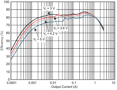
| DCDC1 VO = 0.9 V | PFM Mode | ||
| DFE252012 | 25°C |
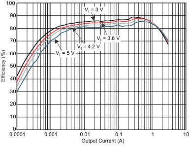
| DCDC1 VO = 1.1375 V | PFM Mode | ||
| DFE252012 | 25°C |
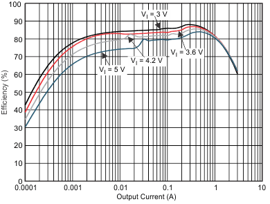
| DCDC1 VO = 1.2 V | PFM Mode | ||
| LQM2NPN-1 µH | 25°C |
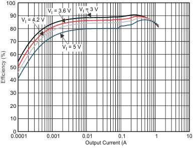
| DCDC2 VO = 1.8 V | PFM Mode | ||
| LQM2NPN-1 µH | 25°C |
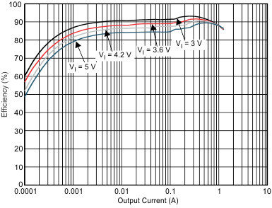
| DCDC2 VO = 2.25 V | PFM Mode | ||
| VLS201612-1 µH | 25°C |
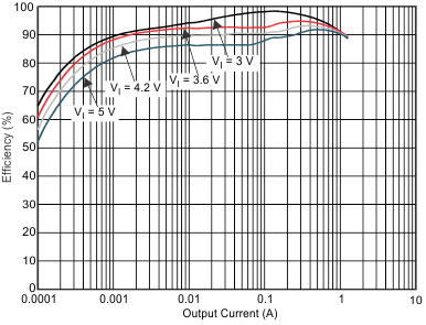
| DCDC2 VO = 2.95 V | PFM Mode | ||
| VLS201612-1 µH | 25°C |
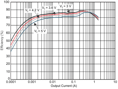
| DCDC3 VO = 1.1375 V | PFM Mode | ||
| DEF252012-1 µH | 25°C |
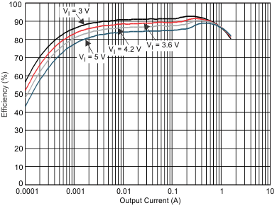
| DCDC3 VO = 2.1 V | PFM Mode | ||
| LQM2NPN-1 µH | 25°C |
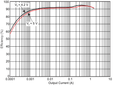
| DCDC3 VO = 3.2 V | PFM Mode | ||
| DEF25012-1 µH | 25°C |
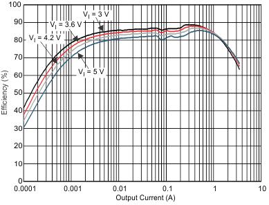
| DCDC4 VO = 1.1375 V | PFM Mode | ||
| DEF25012-1 µH | 25°C |
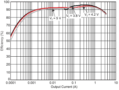
| DCDC4 VO = 3.3 V | PFM Mode | ||
| DEF322512-1 µH | 25°C |
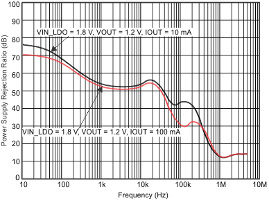
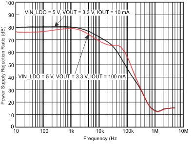 Figure 5-25 LDO4 PSRR vs Frequency
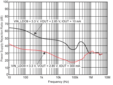 Figure 5-27 LDO9 PSRR vs Frequency
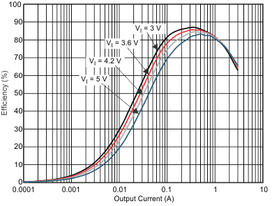
| DCDC1 VO = 0.9 V | PFM Mode | ||
| DFE252012 | 25°C |
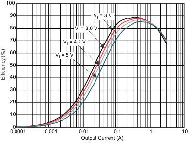
| DCDC1 VO = 1.1375 V | PFM Mode | ||
| DFE252012 | 25°C |
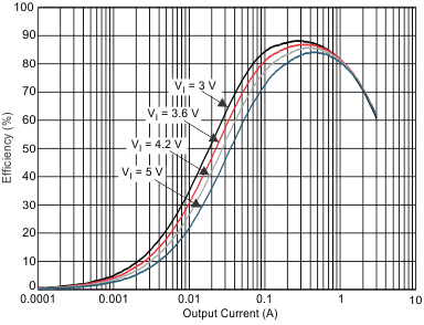
| DCDC1 VO = 1.2 V | PFM Mode | ||
| LQM2NPN-1 µH | 25°C |
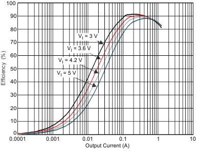
| DCDC2 VO = 1.8 V | PFM Mode | ||
| LQM2NPN-1 µH | 25°C |
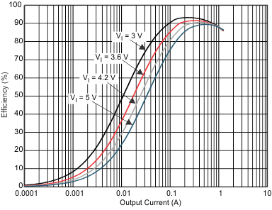
| DCDC2 VO = 2.25 V | PFM Mode | ||
| VLS201612-1 µH | 25°C |
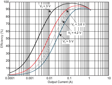
| DCDC2 VO = 2.95 V | PFM Mode | ||
| VLS201612-1 µH | 25°C |
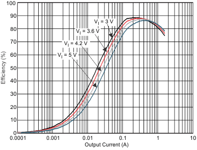
| DCDC3 VO = 1.1375 V | PFM Mode | ||
| DEF252012-1 µH | 25°C |
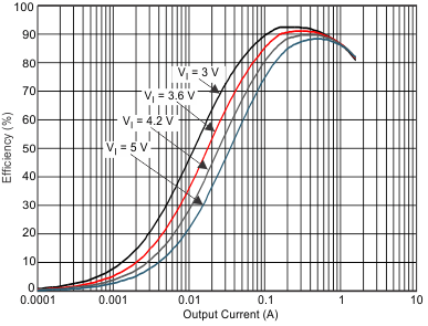
| DCDC3 VO = 2.1 V | PFM Mode | ||
| LQM2NPN-1 µH | 25°C |
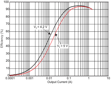
| DCDC3 VO = 3.2 V | PFM Mode | ||
| DEF25012-1 µH | 25°C |
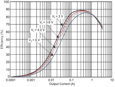
| DCDC4 VO = 1.1375 V | PFM Mode | ||
| DEF322512-1 µH | 25°C |
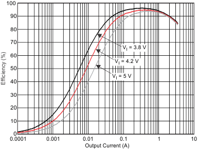
| DCDC4 VO = 3.3 V | PWM Mode | ||
| DEF322512-1 µH | 25°C |
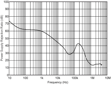
| VIN _LDO = 3.2 V | VOUT = 2.7 V | ||
| IOUT = 225 mA |
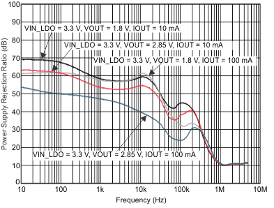 Figure 5-26 LDO6 and LDO8 PSRR vs Frequency