SWCS037I May 2008 – January 2015 TPS65920 , TPS65930
PRODUCTION DATA.
- 1Device Overview
- 2Revision History
- 3Terminal Configuration and Functions
- 4Specifications
-
5Detailed Description
- 5.1
Power Module
- 5.1.1 Power Providers
- 5.1.2 Power References
- 5.1.3 Power Control
- 5.1.4 Power Consumption
- 5.1.5 Power Management
- 5.2 Real-Time Clock and Embedded Power Controller
- 5.3 USB Transceiver
- 5.4 MADC
- 5.5 LED Drivers
- 5.6 Keyboard
- 5.7 Clock Specifications
- 5.8 Debouncing Time
- 5.9 External Components
- 5.1
Power Module
-
6Audio/Voice Module (TPS65930 Device Only)
- 6.1 Audio/Voice Downlink (RX) Module
- 6.2 Audio Uplink (TX) Module
- 7Device and Documentation Support
- 8Mechanical, Packaging, and Orderable Information
Package Options
Mechanical Data (Package|Pins)
- ZCH|139
Thermal pad, mechanical data (Package|Pins)
Orderable Information
4 Specifications
4.1 Absolute Maximum Ratings
| PARAMETER | TEST CONDITIONS | MIN | TYP | MAX | UNIT |
|---|---|---|---|---|---|
| Main battery supply voltage(1) | 2.1 | 4.5 | V | ||
| Voltage on any input | Supply represents the voltage applied to the power supply pin associated with the input | 0.0 | 1.0*Supply | V | |
| Ambient temperature | –40 | 85 | °C | ||
| Junction temperature (TJ) | At 1.4 W (Theta JB 11°C/W 2S2P board) | 105 | °C | ||
| Junction temperature (TJ) for parametric compliance | –40 | 105 | °C | ||
| Storage temperature (Tstg) | –55 | 125 | °C |
4.2 ESD Ratings
| VALUE | UNIT | ||||
|---|---|---|---|---|---|
| VESD | Electrostatic discharge (ESD) performance: | Human body model (HBM), per ANSI/ESDA/JEDEC JS001(1) | All other pins | ±2 | kV |
| CLK32KOUT pin | ±1.5 | ||||
| Charged device model (CDM), per JESD22-C101(2) | ±500 | V | |||
4.3 Recommended Operating Conditions
| MIN | TYP | MAX | UNIT | ||
|---|---|---|---|---|---|
| Main battery supply voltage | 2.7(1) | 3.6 | 4.5 | V | |
| Backup battery supply voltage | 1.8 | 3.2 | 3.3 | V | |
| Ambient temperature range | –40 | 85 | °C | ||
4.4 Thermal Characteristics for ZCH Package
| NAME | DESCRIPTION | TPS65920–2S2P | TPS65920–1S0P | TPS65930–2S2P | TPS65930–1S0P | AIR FLOW (m/s)(2) |
|---|---|---|---|---|---|---|
| (°C/W)(1) | (°C/W) | (°C/W)(1) | (°C/W) | |||
| RΘJC | Junction-to-case (top) | 6.74 | 6.74 | 33.42 | 57.05 | 0.00 |
| RΘJB | Junction-to-board | 13.80 | 14.50 | 13.81 | 14.51 | 0.00 |
| RΘJA | Junction-to-free air | 33.40 | 57.04 | 6.74 | 6.74 | 0.00 |
- JESD51-2, Integrated Circuits Thermal Test Method Environmental Conditions - Natural Convection (Still Air)
- JESD51-3, Low Effective Thermal Conductivity Test Board for Leaded Surface Mount Packages
- JESD51-7, High Effective Thermal Conductivity Test Board for Leaded Surface Mount Packages
- JESD51-9, Test Boards for Area Array Surface Mount Package Thermal Measurements
4.5 Minimum Voltages and Associated Currents
Table 4-1 lists the VBAT minimum and maximum currents per VBAT ball.
Table 4-1 VBAT Minimum Required Per VBAT Ball and Associated Maximum Current
| CATEGORY | PIN AND MODULE | MAXIMUM CURRENT SPECIFIED (mA) | OUTPUT VOLTAGE (V) | VBAT MINIMUM (V) |
|---|---|---|---|---|
| VBAT pin name | VDD_VPLLA3R_IN_6POV | 340 | ||
| Internal module supplied | VPLL1 (LDO) | 40 | 1.0 / 1.2 / 1.3 / 1.8 / 2.8 / 3.0 | Maximum (2.7, output voltage selected + 250 mV) |
| VDD1 core (DCDC) | < 1 | 2.7 | ||
| VDD2 core (DCDC) | < 1 | 2.7 | ||
| SYSPOR (power ref) | < 1 | 2.7 | ||
| PBIAS (power ref) | < 1 | 2.7 | ||
| VBAT pin name | VDD_VDAC_IN_6POV | 370 | ||
| Internal module supplied | VDAC (LDO) | 70 | 1.2 / 1.3 / 1.8 | Maximum (2.7, output voltage selected + 250 mV) |
| VINTANA1 (LDO) | 50 | 1.5 | Maximum (2.7, output voltage selected + 250 mV) |
|
| VINTANA2 (LDO) | 250 | 2.5 / 2.75 | Maximum (2.7, output voltage selected +250 mV) |
|
| VIO core (DCDC) | < 1 | 2.7 | ||
| VBAT pin name | VDD_VAUXI2S_IN_6POV | 350 | ||
| Internal module supplied | VAUX2 (LDO) | 100 | 1.3 / 1.5 / 1.6 / 1.7 / 1.8 / 1.9 / 2.0 / 2.1 / 2.2 / 2.3 / 2.4 / 2.5 / 2.8 | Maximum (2.7, output voltage selected + 250 mV) |
| VBAT pin name | VDD_VMMC1_IN_6POV | 220 | ||
| Internal module supplied | VMMC1 (LDO) | 220 | 1.85 / 2.85 / 3.0 / 3.15 | Maximum (2.7, output voltage selected + 250 mV) |
| Power_REGBATT | 0.001 | 2.7 | ||
| VBAT pin name | VDD_VINT_IN_6POV | 131 | ||
| Internal module supplied | VINTDIG (LDO) | 80 | 1.0 / 1.2 / 1.3 / 1.5 | Maximum (2.7, output voltage selected + 250 mV) |
| VRRTC (LDO) | 30 | 1.5 | Maximum (2.7, output voltage selected + 250 mV) |
|
| VBACKUP (LDO) | 1 | 2.5 / 3.0 / 3.1 / 3.2 | Maximum (2.7, output voltage selected + 250 mV) |
4.6 Digital I/O Electrical Characteristics
Table 4-2 describes the digital I/O electrical characteristics. The following list defines abbreviations used in the table:
- RL: Reference level voltage applied to the I/O cell
- VOL: Low-level output voltage
- VOH: High-level output voltage
- VIL: Low-level input voltage
- VIH: High-level input voltage
- Min: Minimum value
- Max: Maximum value
Table 4-2 Digital I/O Electrical Characteristics
| PIN NAME | VOL (V) | VOH (V) | VIL (V) | VIL (V) | MAX FREQ (MHz) | LOAD (pF) OUTPUT MODE | RISE TIME (ns) | FALL TIME (ns) | ||||
|---|---|---|---|---|---|---|---|---|---|---|---|---|
| MIN | MAX | MIN | MAX | MIN | MAX | MIN | MAX | |||||
| GPIO0/CD1 | 0 | 0.45 | RL–0.45 | RL | 0 | 0.35xRL | 0.65xRL | RL | 33 | 30 | 5.2 | 5.2 |
| JTAG.TDO | ||||||||||||
| GPIO0 | 0 | 0.45 | RL–0.45 | RL | 0 | 0.35xRL | 0.65xRL | RL | 33 | 30 | 5.2 | 5.2 |
| JTAG.TMS | ||||||||||||
| GPIO2 | 0 | 0.45 | RL–0.45 | RL | 0 | 0.35xRL | 0.65xRL | RL | 3 | 30 | 5.2 | 5.2 |
| TEST1 | ||||||||||||
| GPIO15 | 0 | 0.45 | RL–0.45 | RL | 0 | 0.35xRL | 0.65xRL | RL | 3 | 30 | 5.2 | 5.2 |
| TEST2 | ||||||||||||
| GPIO6 | 0 | 0.45 | RL–0.45 | RL | 0 | 0.35xRL | 0.65xRL | RL | 3 | 30 | 5.2 | 5.2 |
| PWM0 | ||||||||||||
| TEST3 | ||||||||||||
| GPIO7 | 0 | 0.45 | RL–0.45 | RL | 0 | 0.35xRL | 0.65xRL | RL | 3 | 30 | 5.2 | 5.2 |
| VIBRA.SYNC | ||||||||||||
| PWM1 | ||||||||||||
| TEST4 | ||||||||||||
| SYSEN | 0 | 0.45 | RL–0.45 | RL | 0 | 0.35×RL | 0.65×RL | RL | 5.2 | 5.2 | ||
| CLKEN | 0 | 0.45 | RL–0.45 | RL | 0 | 0.35×RL | 0.65×RL | RL | 3 | 30 | 33.3 | 33.3 |
| CLKREQ | 0 | 0.45 | RL–0.45 | RL | 0 | 0.35×RL | 0.65×RL | RL | 3 | 33.3 | 33.3 | |
| INT1 | 0 | 0.45 | RL–0.45 | RL | 0 | 0.35×RL | 0.65×RL | RL | 3 | 30 | 33.3 | 33.3 |
| NRESPWRON | 0 | 0.45 | RL–0.45 | RL | 0 | 0.35×RL | 0.65×RL | RL | 3 | 30 | 33.3 | 33.3 |
| NRESWARM | 0 | 0.45 | RL–0.45 | RL | 0 | 0.35×RL | 0.65×RL | RL | 3 | 30 | 33.3 | 33.3 |
| PWRON | 0 | 0.35×1.8V | 0.65×1.8V | VBAT | 3 | 33.3 | 33.3 | |||||
| NSLEEP1 | 0 | 0.45 | RL–0.45 | RL | 0 | 0.35×RL | 0.65×RL | RL | 3 | 33.3 | 33.3 | |
| CLK256FS | 0 | 0.45 | RL–0.45 | RL | 0 | 0.35×RL | 0.65×RL | RL | 12.288 | 30 | 16.3 | 16.3 |
| VMODE1 | 0 | 0.45 | RL–0.45 | RL | 0 | 0.35×RL | 0.65×RL | RL | 3 | 33.3 | 33.3 | |
| BOOT0 | 0 | RL | 3 | 33.3 | 33.3 | |||||||
| BOOT1 | 0 | RL | 3 | 33.3 | 33.3 | |||||||
| REGEN | 0 | 0.45 | RL–0.45 | RL | 0 | 0.35×RL | 0.65×RL | RL | 3 | 30 | 33.3 | 33.3 |
| MSECURE | 0 | 0.45 | RL–0.45 | RL | 0 | 0.35×RL | 0.65×RL | RL | 3 | 33.3 | 33.3 | |
| I2C.SR.SDA | 0 | 0.4 | –0.5 | 0.3×RL | 0.7×RL | RL+0.5 | 3.4 | Up to 400 | ||||
| VMODE2 | 0 | 0.45 | RL–0.45 | RL | 0 | 0.35×RL | 0.65×RL | RL | 3.4 | 29.4 | 29.4 | |
| I2C.SR.SCL | 0 | 0.4 | –0.5 | 0.3×RL | 0.7×RL | RL+0.5 | 3.4 | 10.0 | 10.0 | |||
| I2C.CNTL.SDA | 0 | 0.4 | –0.5 | 0.3×RL | 0.7×RL | RL+0.5 | 3.4 | Up to 400 | ||||
| I2C.CNTL.SCL | 0 | 0.4 | –0.5 | 0.3×RL | 0.7×RL | RL+0.5 | 3.4 | 10.0 | 10.0 | |||
| I2S.CLK | 0 | 0.45 | RL–0.45 | RL | 0 | 0.35×RL | 0.65×RL | RL | 6.5 | 30 | 33.0 | 33.0 |
| I2S.SYNC | 0 | 0.45 | RL–0.45 | RL | 0 | 0.35×RL | 0.65×RL | RL | 6.5 | 30 | 33.0 | 33.0 |
| I2S.DIN | 0 | 0.45 | RL–0.45 | RL | 0 | 0.35×RL | 0.65×RL | RL | 3.25 | 30 | 33.0 | 33.0 |
| I2S.DOUT | 0 | 0.45 | RL–0.45 | RL | 0 | 0.35×RL | 0.65×RL | RL | 3.25 | 30 | 29.0 | 29.0 |
| 32KCLKOUT | 0 | 0.45 | RL–0.45 | RL | 0 | 0.35×RL | 0.65×RL | RL | 0.032 | 30 | 16 | 16 |
| HFCLKOUT | 0 | 0.45 | RL–0.45 | RL | 0 | 0.35×RL | 0.65×RL | RL | 38.4 | 30 | 2.6 | 2.6 |
| UCLK | 0 | 0.45 | RL–0.45 | RL | 0 | 0.35×RL | 0.65×RL | RL | 60 | 10 | 1.0 | 1.0 |
| STP | 0 | 0.45 | RL–0.45 | RL | 0 | 0.35×RL | 0.65×RL | RL | 30 | 10 | 1.0 | 1.0 |
| GPIO9 | ||||||||||||
| DIR | 0 | 0.45 | RL–0.45 | RL | 0 | 0.35×RL | 0.65×RL | RL | 30 | 10 | 1.0 | 1.0 |
| GPIO10 | ||||||||||||
| NXT | 0 | 0.45 | RL–0.45 | RL | 0 | 0.35×RL | 0.65×RL | RL | 30 | 10 | 1.0 | 1.0 |
| GPIO11 | ||||||||||||
| DATA0 | 0 | 0.45 | RL–0.45 | RL | 0 | 0.35×RL | 0.65×RL | RL | 30 | 10 | 1.0 | 1.0 |
| UART4.TXD | ||||||||||||
| DATA1 | 0 | 0.45 | RL–0.45 | RL | 0 | 0.35×RL | 0.65×RL | RL | 30 | 10 | 1.0 | 1.0 |
| UART4.RXD | ||||||||||||
| DATA2 | 0 | 0.45 | RL–0.45 | RL | 0 | 0.35×RL | 0.65×RL | RL | 30 | 10 | 1.0 | 1.0 |
| UART4.RTSI | ||||||||||||
| DATA3 | 0 | 0.45 | RL–0.45 | RL | 0 | 0.35×RL | 0.65×RL | RL | 30 | 10 | 1.0 | 1.0 |
| UART4.CTSO | ||||||||||||
| GPIO12 | 0 | 0.45 | RL–0.45 | RL | 0 | 0.35×RL | 0.65×RL | RL | 30 | 10 | 1.0 | 1.0 |
| DATA4 | 0 | 0.45 | RL–0.45 | RL | 0 | 0.35×RL | 0.65×RL | RL | 30 | 10 | 1.0 | 1.0 |
| GPIO14 | ||||||||||||
| DATA5 | 0 | 0.45 | RL–0.45 | RL | 0 | 0.35×RL | 0.65×RL | RL | 30 | 10 | 1.0 | 1.0 |
| GPIO3 | ||||||||||||
| DATA6 | 0 | 0.45 | RL–0.45 | RL | 0 | 0.35×RL | 0.65×RL | RL | 30 | 10 | 1.0 | 1.0 |
| GPIO4 | ||||||||||||
| DATA7 | 0 | 0.45 | RL–0.45 | RL | 0 | 0.35×RL | 0.65×RL | RL | 30 | 10 | 1.0 | 1.0 |
| GPIO5 | ||||||||||||
| TEST.RESET | 0 | 0.45 | RL–0.45 | RL | 0 | 0.35×RL | 0.65×RL | RL | 3 | 33.0 | 33.0 | |
| TEST | 0 | 0.45 | RL–0.45 | RL | 0 | 0.35×RL | 0.65×RL | RL | 3 | 30 | 29.0 | 29.0 |
| JTAG.TDI/ BERDATA | 0 | 0.45 | RL–0.45 | RL | 0 | 0.35×RL | 0.65×RL | RL | 3 | 33.0 | 33.0 | |
| JTAG.TCK/ BERDATA | 0 | 0.45 | RL–0.45 | RL | 0 | 0.35×RL | 0.65×RL | RL | 3 | 33.0 | 33.0 | |
| GPIO13 | 0 | 0.45 | RL–0.45 | RL | 0 | 0.35×RL | 0.35×RL | 3 | 30 | 33.3 | 33.3 | |
| LEDSYNC | ||||||||||||
| KPD.C0 | 0 | 0.45 | RL–0.45 | RL | 0 | 0.35×RL | 0.65×RL | RL | 0.033 | 30 | 29.0 | 29.0 |
| KPD.C1 | 0 | 0.45 | RL–0.45 | RL | 0 | 0.35×RL | 0.65×RL | RL | 0.033 | 30 | 29.0 | 29.0 |
| KPD.C2 | 0 | 0.45 | RL–0.45 | RL | 0 | 0.35×RL | 0.65×RL | RL | 0.033 | 30 | 29.0 | 29.0 |
| KPD.C3 | 0 | 0.45 | RL–0.45 | RL | 0 | 0.35×RL | 0.65×RL | RL | 0.033 | 30 | 29.0 | 29.0 |
| KPD.C4 | 0 | 0.45 | RL–0.45 | RL | 0 | 0.35×RL | 0.65×RL | RL | 0.033 | 30 | 29.0 | 29.0 |
| KPD.C5 | 0 | 0.45 | RL–0.45 | RL | 0 | 0.35×RL | 0.65×RL | RL | 0.033 | 30 | 29.0 | 29.0 |
| KPD.C6 | 0 | 0.45 | RL–0.45 | RL | 0 | 0.35×RL | 0.65×RL | RL | 0.033 | 30 | 29.0 | 29.0 |
| KPD.C7 | 0 | 0.45 | RL–0.45 | RL | 0 | 0.35×RL | 0.65×RL | RL | 0.033 | 30 | 29.0 | 29.0 |
| KPD.R0 | 0 | 0.45 | RL–0.45 | RL | 0 | 0.35×RL | 0.65×RL | RL | 0.033 | 3051.8 | 3051.8 | |
| KPD.R1 | 0 | 0.45 | RL–0.45 | RL | 0 | 0.35×RL | 0.65×RL | RL | 0.033 | 3051.8 | 3051.8 | |
| KPD.R2 | 0 | 0.45 | RL–0.45 | RL | 0 | 0.35×RL | 0.65×RL | RL | 0.033 | 3051.8 | 3051.8 | |
| KPD.R3 | 0 | 0.45 | RL–0.45 | RL | 0 | 0.35×RL | 0.65×RL | RL | 0.033 | 3051.8 | 3051.8 | |
| KPD.R4 | 0 | 0.45 | RL–0.45 | RL | 0 | 0.35×RL | 0.65×RL | RL | 0.033 | 3051.8 | 3051.8 | |
| KPD.R5 | 0 | 0.45 | RL–0.45 | RL | 0 | 0.35×RL | 0.65×RL | RL | 0.033 | 3051.8 | 3051.8 | |
| KPD.R6 | 0 | 0.45 | 0.45 | RL | 0 | 0.35×RL | 0.65×RL | RL | 0.033 | 3051.8 | 3051.8 | |
| KPD.R7 | 0 | 0.45 | 0.45 | RL | 0 | 0.35×RL | 0.65×RL | RL | 0.033 | 3051.8 | 3051.8 | |
4.7 Timing Requirements and Switching Characteristics
4.7.1 Timing Parameters
The timing parameter symbols used in the timing requirement and switching characteristic tables are created in accordance with JEDEC Standard 100. To shorten the symbols, some pin names and other related terminologies are abbreviated, as shown in Table 4-3.
Table 4-3 Timing Parameters
| SUBSCRIPTS | |
|---|---|
| SYMBOL | PARAMETER |
| c | Cycle time (period) |
| d | Delay time |
| dis | Disable time |
| en | Enable time |
| h | Hold time |
| su | Setup time |
| START | Start bit |
| t | Transition time |
| v | Valid time |
| w | Pulse duration (width) |
| X | Unknown, changing, or don't care level |
| H | High |
| L | Low |
| V | Valid |
| IV | Invalid |
| AE | Active edge |
| FE | First edge |
| LE | Last edge |
| Z | High impedance |
4.7.2 Target Frequencies
Table 4-4 assumes testing over the recommended operating conditions.
Table 4-4 TPS65920/TPS65930 Interface Target Frequencies
| I/O INTERFACE | INTERFACE DESIGNATION | TARGET FREQUENCY | |
|---|---|---|---|
| 1.5 V | |||
| SmartReflex inter-integrated circuit (I2C) | I2C | Slave HS mode | 3.6 Mbps |
| General-purpose I2C | Slave fast-speed mode | 400 Kbps | |
| Slave standard mode | 100 Kbps | ||
| USB | USB | HS | 480 Mbps |
| FS | 12 Mbps | ||
| LS | 1.5 Mbps | ||
| JTAG | RealView ICE tool | 30 MHz | |
| XDS560 and XDS510 tools | 30 MHz | ||
| Lauterbach tool | 30 MHz | ||
| TDM/inter-IC sound (I2S) | I2S | 1/(64 * Fs)(1) | |
| Right-justified | 1/(64 * Fs)(1) | ||
| Left-justified | 1/(64 * Fs)(1) | ||
| TDM | 1/(128 * Fs)(1) | ||
| Voice/Bluetooth pulse code modulation (PCM) interface | PCM (master mode) | 1/(65 * Fs)(2) | |
| PCM (slave mode) | 1/(33 to 65 * Fs)(2) | ||
4.7.3 I2C Timing
The TPS65920/TPS65930 device provides two I2C HS slave interfaces (one for general-purpose and one for SmartReflex). These interfaces support standard mode (100 Kbps), fast mode (400 Kbps), and HS mode (3.4 Mbps). The general-purpose I2C module embeds four slave hard-coded addresses (ID1 = 48h, ID2 = 49h, ID3 = 4Ah, and ID4 = 4Bh). The SmartReflex I2C module uses one slave hard-coded address (ID5). The master mode is not supported.
Table 4-5 and Table 4-6 assume testing over the recommended operating conditions (see Figure 4-1).
 Figure 4-1 I2C Interface—Transmit and Receive in Slave Mode
Table 4-5 I2C Interface—Timing Requirements(1)(2)
| NOTATION | PARAMETER | MIN | MAX | UNIT | |
|---|---|---|---|---|---|
| Slave HS Mode | |||||
| I3 | tsu(SDA-SCLH) | Setup time, SDA valid to SCL high | 10 | ns | |
| I4 | th(SCLL-SDA) | Hold time, SDA valid from SCL low | 0 | 70 | ns |
| I7 | tsu(SCLH-SDAL) | Setup time, SCL high to SDA low | 160 | ns | |
| I8 | th(SDAL-SCLL) | Hold time, SCL low from SDA low | 160 | ns | |
| I9 | tsu(SDAH-SCLH) | Setup time, SDA high to SCL high | 160 | ns | |
| Slave Fast-Speed Mode | |||||
| I3 | tsu(SDA-SCLH) | Setup time, SDA valid to SCL high | 100 | ns | |
| I4 | th(SCLL-SDA) | Hold time, SDA valid from SCL low | 0 | 0.9 | ns |
| I7 | tsu(SCLH-SDAL) | Setup time, SCL high to SDA low | 0.6 | ns | |
| I8 | th(SDAL-SCLL) | Hold time, SCL low from SDA low | 0.6 | ns | |
| I9 | tsu(SDAH-SCLH) | Setup time, SDA high to SCL high | 0.6 | ns | |
| Slave Standard Mode | |||||
| I3 | tsu(SDA-SCLH) | Setup time, SDA valid to SCL high | 250 | ns | |
| I4 | th(SCLL-SDA) | Hold time, SDA valid from SCL low | 0 | ns | |
| I7 | tsu(SCLH-SDAL) | Setup time, SCL high to SDA low | 4.7 | ns | |
| I8 | th(SDAL-SCLL) | Hold time, SCL low from SDA low | 4 | ns | |
| I9 | tsu(SDAH-SCLH) | Setup time, SDA high to SCL high | 4 | ns | |
80 ns in HS mode (3.4 Mbps)
300 ns in fast-speed mode (400 Kbps)
1000 ns in standard mode (100 Kbps)
SCL is equal to I2C.SR.SCL or I2C.CNTL.SCL.
Table 4-6 lists the switching requirements of the I2C interface.
Table 4-6 I2C Interface—Switching Requirements(1)(2)
| NOTATION | PARAMETER | MIN | MAX | UNIT | |
|---|---|---|---|---|---|
| Slave HS Mode | |||||
| I1 | tw(SCLL) | Pulse duration, SCL low | 160 | ns | |
| I2 | tw(SCLH) | Pulse duration, SCL high | 60 | ns | |
| Slave Fast-Speed Mode | |||||
| I1 | tw(SCLL) | Pulse duration, SCL low | 1.3(3) | µs | |
| I2 | tw(SCLH) | Pulse duration, SCL high | 0.6 | µs | |
| Slave Standard Mode | |||||
| I1 | tw(SCLL) | Pulse duration, SCL low | 4.7 | µs | |
| I2 | tw(SCLH) | Pulse duration, SCL high | 4 | µs | |
100 pF in HS mode (3.4 Mbps)
400 pF in fast-speed mode (400 Kbps)
400 pF in standard mode (100 Kbps)
SCL is equal to I2C.SR.SCL or I2C.CNTL.SCL
4.7.4 Audio Interface: TDM/I2S Protocol
The TPS65920/TPS65930 device acts as a master for the TDM and I2S interfaces or as a slave for only the I2S interface. If the TPS65920/TPS65930 device is the master, it must provide the frame synchronization (TDM/I2S_SYNC) and bit clock (TDM/I2S_CLK) to the host processor. If it is the slave, the TPS65920/TPS65930 device receives frame synchronization and the bit clock.
The TPS65920/TPS65930 device supports the I2S, TDM, left-justified, and right-justified data formats, but does not support TDM slave mode.
4.7.4.1 I2S Right- and Left-Justified Data Format
Table 4-7 and Table 4-8 assume testing over the recommended operating conditions (see Figure 4-2 and Figure 4-3).
 Figure 4-2 I2S Interface—I2S Master ModeI
 Figure 4-3 I2S Interface—I2S Slave Mode
The timing requirements listed in Table 4-7 are valid on the following conditions of input slew and output load:
- Rise and fall time range of inputs (SYNC, DIN) is tR/tF = 1.0 ns/6.5 ns
- Capacitance load range of outputs (CLK, SYNC, DOUT) is CLoad = 1 pF/30 pF
The input timing requirements in Table 4-7 are given by considering a rising or falling time of 6.5 ns.
Table 4-7 I2S Interface—Timing Requirements
| NOTATION | PARAMETER | MIN | MAX | UNIT | |
|---|---|---|---|---|---|
| Master Mode | |||||
| I3 | tsu(DIN-CLKH) | Setup time, I2S.DIN valid to I2S.CLK high2 | 25 | ns | |
| I4 | th(DIN-CLKH) | Hold time, I2S.DIN valid from I2S.CLK high. | 0 | ns | |
| Slave Mode | |||||
| I0 | tc(CLK) | Cycle time, I2S.CLK(1) | 1/64 * Fs | ns | |
| I1 | tw(CLK) | Pulse duration, I2S.CLK high or low(2) | 0.45 * P | 0.55 * P | ns |
| I3 | tsu(DIN-CLKH) | Setup time, I2S.DIN valid to I2S.CLK high | 5 | ns | |
| I4 | th(DIN-CLKH) | Hold time, I2S.DIN valid from I2S.CLK high. | 5 | ns | |
| I6 | tsu(SYNC-CLKH) | Setup time, I2S.SYNC valid to I2S.CLK high | 5 | ns | |
| I7 | th(SYNC-CLKH) | Hold time, I2S.SYNC valid from I2S.CLK high | 5 | ns | |
The capacitive load for Table 4-8 is 7 pF. Table 4-8 lists the switching characteristics for the I2S interface.
Table 4-8 I2S Interface—Switching Characteristics
| NOTATION | PARAMETER | MIN | MAX | UNIT | |
|---|---|---|---|---|---|
| Master Mode | |||||
| I0 | tc(CLK) | Cycle time, I2S.CLK(1) | 1/64 * Fs | ns | |
| I1 | tw(CLK) | Pulse duration, I2S.CLK high or low(2) | 0.45 * P | 0.55 * P | ns |
| I2 | td(CLKL-SYNC) | Delay time, I2S.CLK falling edge to I2S.SYNC transition | –10 | 10 | ns |
| I5 | td(CLKL-DOUT) | Delay time, I2S.CLK falling edge to I2S.DOUT transition | –10 | 10 | ns |
| Slave Mode | |||||
| I5 | td(CLKL-DOUT) | Delay time, I2S.CLK falling edge to I2S.DOUT transition | 0 | 20 | ns |
4.7.4.2 TDM Data Format
Table 4-9 and Table 4-10 assume testing over the recommended operating conditions (see Figure 4-4).
 Figure 4-4 TDM Interface—TDM Master Mode
The timing requirements listed in Table 4-9 are valid on the following conditions of input slew and output load:
- Rise and fall time range of inputs (SYNC, DIN) is tR/tF = 1.0 ns/6.5 ns
- Capacitance load range of outputs (CLK, SYNC, DOUT) is CLoad = 1 pF/30 pF
Table 4-9 TDM Interface Master Mode—Timing Requirements
| NOTATION | PARAMETER | MIN | MAX | UNIT | |
|---|---|---|---|---|---|
| T3 | tsu(DIN-CLKH) | Setup time, TDM.DIN valid to TDM.CLK high | 25 | ns | |
| T4 | th(DIN-CLKH) | Hold time, TDM.DIN valid from TDM.CLK high | 0 | ns | |
Table 4-10 lists the switching characteristics of the TDM interface master mode.
Table 4-10 TDM Interface Master Mode—Switching Characteristics
| NOTATION | PARAMETER | MIN | MAX | UNIT | |
|---|---|---|---|---|---|
| T0 | tc(CLK) | Cycle time, TDM.CLK (1) | 1/64 * Fs | ns | |
| T1 | tw(CLK) | Pulse duration, TDM.CLK high or low(2) | 0.45*P | 0.55*P | ns |
| T2 | td(CLKL-SYNC) | Delay time, TDM.CLK rising edge to TDM.SYNC transition | –10 | 10 | ns |
| T5 | td(CLKL-DOUT) | Delay time, TDM.CLK rising edge to TDM.DOUT transition | –10 | 12 | ns |
4.7.5 JTAG Interfaces
The TPS65920/TPS65930 device JTAG TAP controller handles standard IEEE JTAG interfaces. This section describes the timing requirements for the tools used to test TPS65920/TPS65930 device power management.
The JTAG/TAP module provides a JTAG interface according to IEEE Std1149.1a. This interface uses the four I/O pins TMS, TCK, TDI, and TDO. The TMS, TCK, and TDI inputs contain a pullup device, which makes their state high when they are not driven. The output TDO is a 3-state output, which is high impedance except when data are shifted between TDI and TDO.
- TCK is the test clock signal.
- TMS is the test mode select signal.
- TDI is the scan path input.
- TDO is the scan path output.
TMS and TDO are multiplexed at the top level with the GPIO0 and GPIO1 pins. The dedicated external TEST pin switches from functional mode (GPIO0/GPIO1) to JTAG mode (TMS/TDO). The JTAG operations are controlled by a state-machine that follows the IEEE Std1149.1a state diagram. This state-machine is reset by the TPS65920/TPS65930 internal power-on reset (POR). A test mode is selected by writing a 6-bit word (instruction) into the instruction register and then accessing the related data register.
Table 4-11 and Table 4-12 assume testing over the recommended operating conditions (see Figure 4-5).
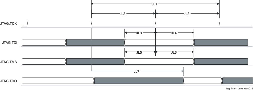 Figure 4-5 JTAG Interface Timing
The input timing requirements are given by considering a rising or falling edge of 7 ns.
Table 4-11 JTAG Interface—Timing Requirements
| NOTATION | PARAMETER | MIN | MAX | UNIT | |
|---|---|---|---|---|---|
| Clock | |||||
| JL1 | tc(TCK) | Cycle time, JTAG.TCK period | 30 | ns | |
| JL2 | tw(TCK) | Pulse duration, JTAG.TCK high or low(1) | 0.48*P | 0.52*P | ns |
| Read Timing | |||||
| JL3 | tsu(TDIV-TCKH) | Setup time, JTAG.TDI valid before JTAG.TCK high | 8 | ns | |
| JL4 | th(TDIV-TCKH) | Hold time, JTAG.TDI valid after JTAG.TCK high | 5 | ns | |
| JL5 | tsu(TMSV-TCKH) | Setup time, JTAG.TMS valid before JTAG.TCK high | 8 | ns | |
| JL6 | th(TMSV-TCKH) | Hold time, JTAG.TMS valid after JTAG.TCK high | 5 | ns | |
The capacitive load is 35 pF.
Table 4-12 JTAG Interface—Switching Characteristics
| NOTATION | PARAMETER | MIN | MAX | UNIT | |
|---|---|---|---|---|---|
| Write Timing | |||||
| JL7 | td(TCK-TDOV)) | Delay time, JTAG, TCK active edge to JTAG.TDO valid | 0 | 14 | ns |