SLVSEW8B August 2019 – December 2019 TPS66020 , TPS66021
PRODUCTION DATA.
- 1 Features
- 2 Applications
- 3 Description
- 4 Revision History
- 5 Pin Configuration and Functions
-
6 Specifications
- 6.1 Absolute Maximum Ratings
- 6.2 ESD Ratings
- 6.3 Recommended Operating Conditions
- 6.4 Recommended Supply Load Capacitance
- 6.5 Thermal Information
- 6.6 PP5V Power Switch Characteristics
- 6.7 PPHV Power Switch Characteristics
- 6.8 Power Path Supervisory
- 6.9 VBUS LDO Characteristics
- 6.10 Thermal Shutdown Characteristics
- 6.11 Input-output (I/O) Characteristics
- 6.12 Power Consumption Characteristics
- 6.13 Typical Characteristics
- 7 Parameter Measurement Information
-
8 Detailed Description
- 8.1 Overview
- 8.2 Functional Block Diagram
- 8.3 Feature Description
- 8.4 Device Functional Modes
-
9 Application and Implementation
- 9.1 Application Information
- 9.2
Typical Application
- 9.2.1 Design Requirements
- 9.2.2
Detailed Design Procedure
- 9.2.2.1 External Current Reference Resistor (RIREF)
- 9.2.2.2 External VLDO Capacitor (CVLDO)
- 9.2.2.3 PP5V Power Path Capacitance
- 9.2.2.4 PPHV, VBUS Power Path Capacitance
- 9.2.2.5 VBUS TVS Protection (Optional)
- 9.2.2.6 VBUS Schottky Diode Protection (Optional)
- 9.2.2.7 VBUS Overvoltage Protection (Optional)
- 9.2.2.8 Dead Battery Support
- 9.2.2.9 Fast Role Swap (FRS) (Optional)
- 9.2.3 Application Curves
- 10Power Supply Recommendations
- 11Layout
- 12Device and Documentation Support
- 13Mechanical, Packaging, and Orderable Information
Package Options
Mechanical Data (Package|Pins)
- YBG|28
Thermal pad, mechanical data (Package|Pins)
Orderable Information
8.3.5.1 Supply Connections
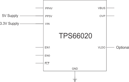
Figure 15 shows the TPS66020 VIN being supplied from a 3.3-V supply. The VLDO output may or may not be used to supply other circuitry in the application, for example a PD Controller. During a dead battery condition, the internal 3.3-V VBUS LDO provides power to the TPS66020 and the VLDO output. Once VIN input supply becomes available, the VBUS LDO is disabled and VIN provides power to the VLDO output.
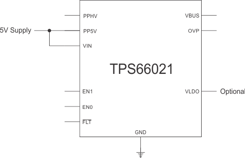
The TPS66021 is well suited for 5 V only systems. VIN of the TPS66021 may be powered from an independent supply, but in most applications it will be connected to the PP5V supply. Figure 16 shows where the VIN supply is shared with PP5V. The VLDO output may be used optionally to supply power to external circuitry. During a dead battery condition, the internal 5-V VBUS LDO provides power to the TPS66021 and the VLDO output. Once the VIN input supply, in this case PP5V, becomes available, the VBUS LDO is disabled and PP5V provides power to the VLDO output.
 Figure 15. TPS66020 VIN 3.3-V Supply
  Figure 16. TPS66021 VIN 5-V Shared Supply