SBVS278A February 2016 – October 2016 TPS720-Q1
PRODUCTION DATA.
- 1 Features
- 2 Applications
- 3 Description
- 4 Revision History
- 5 Pin Configuration and Functions
- 6 Specifications
- 7 Detailed Description
- 8 Application and Implementation
- 9 Power Supply Recommendations
- 10Layout
- 11Device and Documentation Support
- 12Mechanical, Packaging, and Orderable Information
Package Options
Mechanical Data (Package|Pins)
- DRV|6
Thermal pad, mechanical data (Package|Pins)
- DRV|6
Orderable Information
7 Detailed Description
7.1 Overview
The TPS720-Q1 family of LDO regulators uses innovative circuitry to achieve ultra-wide bandwidth and high loop gain, resulting in extremely high PSRR (up to 1 MHz) at very low headroom (VIN – VOUT). The implementation of the BIAS pin on the TPS720-Q1 vastly improves efficiency of low VOUT applications by allowing the use of a pre-regulated, low-voltage input supply. The TPS720-Q1 supports a novel feature where the output of the LDO regulates under light loads (< 500 μA) when the IN pin is left floating. The light-load drive current is sourced from VBIAS under this condition. This feature is particularly useful in power-saving applications where the dc-dc converter connected to the IN pin is disabled but the LDO is still required to regulate the voltage to a light load. These features, combined with low noise, low ground pin current, and ultra-small packaging, make this device ideal for portable applications. This family of regulators offers sub-band-gap output voltages, current limit, and thermal protection, and is fully specified from –40°C to +125°C.
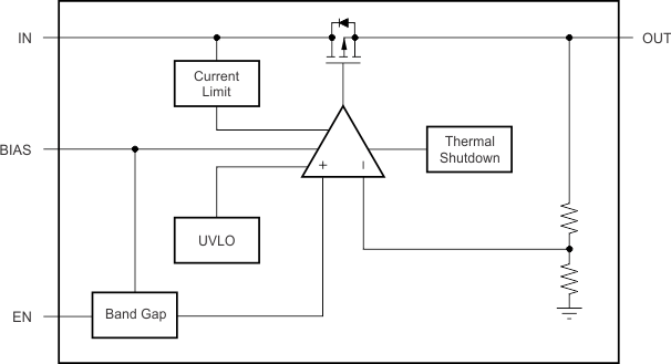
7.2 Functional Block Diagram

7.3 Feature Description
7.3.1 Internal Current Limit
The TPS720-Q1 internal current limits help protect the regulator during fault conditions. During current limit, the output sources a fixed amount of current that is largely independent of output voltage. In such a case, the output voltage is not regulated, and is VOUT = ILIMIT × RLOAD. The NMOS pass transistor dissipates (VIN – VOUT) × IOUT until thermal shutdown is triggered and the device is turned off. When the device cools down, the internal thermal shutdown circuit turns the device back on. If the fault condition continues, the device cycles between current limit and thermal shutdown; see Thermal Considerations for more details.
The NMOS pass element in the TPS720-Q1 has a built-in body diode that conducts current when the voltage at OUT exceeds the voltage at IN. This current is not limited, so if extended reverse voltage operation is anticipated, TI recommends external limiting to 5% of rated output current.
7.3.2 Inrush Current Limit
The TPS720-Q1 family of LDO regulators implements a novel inrush current limit circuit architecture: the current drawn through the IN pin is limited to a finite value. This IINRUSHLIMIT charges the output to the final voltage. All current drawn through VIN charges the output capacitance when the load is disconnected. Equation 1 shows the inrush current limit performed by the circuit.

Assuming a COUT of 2.2 μF with the load disconnected (that is, ILOAD = 0), the IINRUSHLIMIT is calculated to be 100 mA. The inrush current charges the LDO output capacitor. If the output of the LDO regulates to 1.3 V, then the LDO charges the output capacitor to the final output value in approximately 28.6 μs.
Another consideration is when a load is connected to the output of an LDO. The TPS720-Q1 inrush current limit circuit employs a technique that supplies not only the IINRUSHLIMIT, but the additional current required by the load. If ILOAD = 350 mA, then IINRUSHLIMIT calculates to be approximately 450 mA (from Equation 1).
7.3.3 Shutdown
The enable pin (EN) is active high and is compatible with standard and low-voltage, TTL-CMOS levels. When shutdown capability is not required, EN can be connected to the IN pin.
7.3.4 Undervoltage Lockout (UVLO)
The TPS720-Q1 uses an undervoltage lockout circuit on the BIAS pin to keep the output shut off until the internal circuitry is operating properly. The UVLO circuit has a deglitch feature that typically ignores undershoot transients on the input if these transients are less than 50 μs in duration.
7.4 Device Functional Modes
Driving the EN pin over 1.1 V turns on the regulator. Driving the EN pin below 0.4 V causes the regulator to enter shutdown mode. In shutdown, the current consumption of the device is typically reduced to 500 nA.