SBVS252B October   2014  – February 2019 TPS735-Q1

PRODUCTION DATA.  

  1. Features
  2. Applications
  3. Description
    1.     Device Images
      1.      Typical Application
  4. Revision History
  5. Pin Configuration and Functions
    1.     Pin Functions
  6. Specifications
    1. 6.1 Absolute Maximum Ratings
    2. 6.2 ESD Ratings
    3. 6.3 Recommended Operating Conditions
    4. 6.4 Thermal Information
    5. 6.5 Electrical Characteristics
    6. 6.6 Typical Characteristics
  7. Detailed Description
    1. 7.1 Overview
    2. 7.2 Functional Block Diagram
    3. 7.3 Feature Description
      1. 7.3.1 Internal Current-Limit
      2. 7.3.2 Shutdown
      3. 7.3.3 Dropout Voltage
      4. 7.3.4 Startup and Noise Reduction Capacitor
      5. 7.3.5 Transient Response
      6. 7.3.6 Undervoltage Lockout (UVLO)
      7. 7.3.7 Minimum Load
    4. 7.4 Device Functional Modes
      1. 7.4.1 Normal Operation
      2. 7.4.2 Dropout Operation
      3. 7.4.3 Disabled
  8. Application and Implementation
    1. 8.1 Application Information
    2. 8.2 Typical Application
      1. 8.2.1 Design Requirements
        1. 8.2.1.1 Input and Output Capacitor Requirements
        2. 8.2.1.2 Feedback Capacitor Requirements (TPS73501-Q1 only)
      2. 8.2.2 Detailed Design Procedure
        1. 8.2.2.1 Output Noise
      3. 8.2.3 Application Curves
  9. Power Supply Recommendations
  10. 10Layout
    1. 10.1 Layout Guidelines
      1. 10.1.1 Board Layout Recommendations to Improve PSRR and Noise Performance
      2. 10.1.2 Thermal Protection
      3. 10.1.3 Package Mounting
      4. 10.1.4 Power Dissipation
      5. 10.1.5 Estimating Junction Temperature
    2. 10.2 Layout Example
  11. 11Device and Documentation Support
    1. 11.1 Device Support
      1. 11.1.1 Device Nomenclature
    2. 11.2 Documentation Support
      1. 11.2.1 Related Documentation
    3. 11.3 Receiving Notification of Documentation Updates
    4. 11.4 Community Resources
    5. 11.5 Trademarks
    6. 11.6 Electrostatic Discharge Caution
    7. 11.7 Glossary
  12. 12Mechanical, Packaging, and Orderable Information

Package Options

Mechanical Data (Package|Pins)
Thermal pad, mechanical data (Package|Pins)
Orderable Information

Estimating Junction Temperature

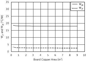
Using the thermal metrics ΨJT and ΨJB, as shown in the table, the junction temperature can be estimated with the corresponding formulas (given in Equation 5).

Equation 5. TPS735-Q1 eq_05_slvscd4.gif

where

  • PD is the power dissipation calculated with Equation 2,
  • TT is the temperature at the center-top of the device package, and
  • TB is the PCB temperature measured 1 mm away from the device package on the PCB surface (as shown in Figure 23).
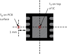
TPS735-Q1 ai_thermal_measmt_drb_slvscd4.gifFigure 23. Measuring Points for TT and TB

NOTE

Both TT and TB can be measured on actual application boards using an infrared thermometer.

For more information about measuring TT and TB, see the application note, Using New Thermal Metrics, SBVA025.

According to Figure 24, the thermal metrics (ΨJT and ΨJB) have very little dependency on copper area. Using ΨJT or ΨJB with Equation 5 is a good way to estimate TJ by simply measuring TT or TB on an application board.
TPS735-Q1 ai_psi_jt_jb_slvscd4.gifFigure 24. ΨJT and ΨJB vs Board Size