SBVS442 December 2022 TPS748A
PRODUCTION DATA
- 1 Features
- 2 Applications
- 3 Description
- 4 Revision History
- 5 Pin Configuration and Functions
- 6 Specifications
- 7 Detailed Description
- 8 Application and Implementation
- 9 Device and Documentation Support
- 10Mechanical, Packaging, and Orderable Information
Package Options
Mechanical Data (Package|Pins)
- DRC|10
Thermal pad, mechanical data (Package|Pins)
- DRC|10
Orderable Information
8.1.2 Dropout Voltage
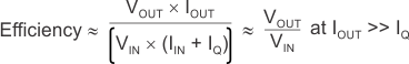
The TPS748A offers very low dropout performance, making the device designed for high-current, low VIN and low VOUT applications. The low dropout allows the device to be used in place of a dc/dc converter and still achieve good efficiency. Equation 4 provides a quick estimate of the efficiency.
This efficiency provides designers with the power architecture for applications to achieve the smallest, simplest, and lowest cost solutions.
For this architecture, there are two different specifications for dropout voltage. The first specification (see Figure 6-11 ) is referred to as VIN dropout and is used when an external bias voltage is applied to achieve low dropout. This specification assumes that VBIAS is at least 2.8 V above VOUT, which is the case for VBIAS when powered by a 5.0-V rail with 5% tolerance and with VOUT = 1.5 V. If VBIAS is higher than VOUT + 2.8 V, the VIN dropout is less than specified.
The second specification (illustrated in Figure 6-12 ) is referred to as VBIAS dropout and applies to applications where IN and BIAS are tied together. This option allows the device to be used in applications where an auxiliary bias voltage is not available or low dropout is not required. Dropout is limited by BIAS in these applications because VBIAS provides the gate drive to the pass transistor; therefore, VBIAS must be 1.9 V above VOUT. Because of this usage, having IN and BIAS tied together become a highly inefficient solution that can consume large amounts of power. Pay attention not to exceed the power rating of the device package.