SBVS056L January 2005 – February 2022 TPS799
PRODUCTION DATA
- 1 Features
- 2 Applications
- 3 Description
- 4 Revision History
- 5 Pin Configuration and Functions
- 6 Specifications
- 7 Detailed Description
- 8 Application and Implementation
- 9 Power Supply Recommendations
- 10Layout
- 11Device and Documentation Support
- 12Mechanical, Packaging, and Orderable Information
Package Options
Mechanical Data (Package|Pins)
Thermal pad, mechanical data (Package|Pins)
- DRV|6
Orderable Information
3 Description
The TPS799 low-dropout (LDO), low-power linear regulator offers excellent ac performance with very low ground current. High power-supply rejection ratio (PSRR), low noise, fast start-up, and excellent line and load transient response are provided while consuming a very low 40-μA (typical) ground current.
The TPS799 is stable with ceramic capacitors and uses an advanced BiCMOS fabrication process to yield a dropout voltage of typically 100 mV at a 200-mA output. The TPS799 uses a precision voltage reference and feedback loop to achieve an overall accuracy of 2% over all load, line, process, and temperature variations. The TPS799 features inrush current protection when the EN toggle is used to start the device, immediately clamping the current.
This device is fully specified over the temperature range of TJ = –40°C to +125°C, and is offered in a low-profile, die-sized ball grid array (DSBGA) package, making this device a good choice for wireless handsets and WLAN cards. This device is also offered in 5-pin SOT-23-THIN and 6-pin WSON packages.
| PART NUMBER | PACKAGE | BODY SIZE (NOM) |
|---|---|---|
| TPS799 | SOT-23-THIN (5) | 2.90 mm × 1.60 mm |
| WSON (6) | 2.00 × 2.00 mm | |
| DSBGA (5) | 1.34 mm × 0.97 mm |
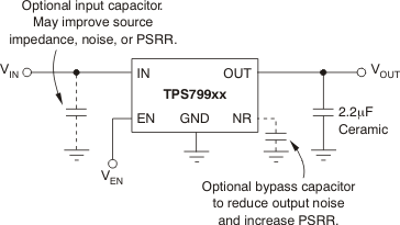
 Typical Application Circuit:
Fixed Voltage Versions
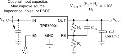
 Typical Application Circuit:
Adjustable Voltage Version