SBVS316B September 2018 – December 2020 TPS7A11
PRODUCTION DATA
- 1 Features
- 2 Applications
- 3 Description
- 4 Revision History
- 5 Pin Configuration and Functions
- 6 Specifications
- 7 Detailed Description
-
8 Application and Implementation
- 8.1
Application Information
- 8.1.1 Recommended Capacitor Types
- 8.1.2 Input and Output Capacitor Requirements
- 8.1.3 Load Transient Response
- 8.1.4 Dropout Voltage
- 8.1.5 Behavior During Transition From Dropout Into Regulation
- 8.1.6 Undervoltage Lockout Circuit Operation
- 8.1.7 Power Dissipation (PD)
- 8.1.8 Estimating Junction Temperature
- 8.1.9 Recommended Area for Continuous Operation
- 8.2 Typical Application
- 8.1
Application Information
- 9 Power Supply Recommendations
- 10Layout
- 11Device and Documentation Support
Package Options
Mechanical Data (Package|Pins)
Thermal pad, mechanical data (Package|Pins)
- DRV|6
Orderable Information
8.1.6 Undervoltage Lockout Circuit Operation
The VIN UVLO circuit makes sure that the device remains disabled before the input supply reaches the minimum operational voltage range. The VIN UVLO circuit also makes sure that the device shuts down when the input supply collapses. Similarly, the VBIAS UVLO circuit makes sure that the device stays disabled before the bias supply reaches the minimum operational voltage range. The VBIAS UVLO circuit also makes sure that the device shuts down when the bias supply collapses.
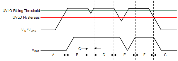
Figure 8-2 depicts the UVLO circuit response to various input or bias voltage events. The diagram can be separated into the following parts:
- Region A: The device does not start until the input or bias voltage reaches the UVLO rising threshold
- Region B: Normal operation, regulating device
- Region C: Brownout event above the UVLO falling threshold (UVLO rising threshold – UVLO hystersis). The output may fall out of regulation but the device is still enabled.
- Region D: Normal operation, regulating device
- Region E: Brownout event below the UVLO falling threshold. The device is disabled in most cases and the output falls as a result of the load and active discharge circuit. The device is re-enabled when the UVLO rising threshold is reached and a normal start-up follows.
- Region F: Normal operation followed by the input or bias falling to the UVLO falling threshold
- Region G: The device is disabled when the input or bias voltages fall below the UVLO falling threshold to 0 V. The output falls as a result of the load and active discharge circuit.
 Figure 8-2 Typical VIN or VBIAS UVLO Circuit Operation