SBVS290B December   2018  – October 2019 TPS7A26

PRODUCTION DATA.  

  1. Features
  2. Applications
  3. Description
    1.     Device Images
      1.      Typical Application Circuit
  4. Revision History
  5. Pin Configuration and Functions
    1.     Pin Functions
  6. Specifications
    1. 6.1 Absolute Maximum Ratings
    2. 6.2 ESD Ratings
    3. 6.3 Recommended Operating Conditions
    4. 6.4 Thermal Information
    5. 6.5 Electrical Characteristics
    6. 6.6 Typical Characteristics
  7. Detailed Description
    1. 7.1 Overview
    2. 7.2 Functional Block Diagram
    3. 7.3 Feature Description
      1. 7.3.1 Output Enable
      2. 7.3.2 Dropout Voltage
      3. 7.3.3 Current Limit
      4. 7.3.4 Undervoltage Lockout (UVLO)
      5. 7.3.5 Thermal Shutdown
      6. 7.3.6 Power Good
      7. 7.3.7 Active Overshoot Pulldown Circuitry
    4. 7.4 Device Functional Modes
      1. 7.4.1 Device Functional Mode Comparison
      2. 7.4.2 Normal Operation
      3. 7.4.3 Dropout Operation
      4. 7.4.4 Disabled
  8. Application and Implementation
    1. 8.1 Application Information
      1. 8.1.1 Adjustable Device Feedback Resistors
      2. 8.1.2 Recommended Capacitor Types
      3. 8.1.3 Input and Output Capacitor Requirements
      4. 8.1.4 Reverse Current
      5. 8.1.5 Feed-Forward Capacitor (CFF)
      6. 8.1.6 Power Dissipation (PD)
      7. 8.1.7 Estimating Junction Temperature
      8. 8.1.8 Special Consideration for Line Transient
    2. 8.2 Typical Application
      1. 8.2.1 Design Requirements
      2. 8.2.2 Detailed Design Procedure
        1. 8.2.2.1 Transient Response
        2. 8.2.2.2 Selecting Feedback Divider Resistors
        3. 8.2.2.3 Thermal Dissipation
      3. 8.2.3 Application Curve
  9. Power Supply Recommendations
  10. 10Layout
    1. 10.1 Layout Guidelines
    2. 10.2 Layout Examples
  11. 11Device and Documentation Support
    1. 11.1 Device Support
      1. 11.1.1 Device Nomenclature
    2. 11.2 Documentation Support
      1. 11.2.1 Related Documentation
    3. 11.3 Receiving Notification of Documentation Updates
    4. 11.4 Community Resources
    5. 11.5 Trademarks
    6. 11.6 Electrostatic Discharge Caution
    7. 11.7 Glossary
  12. 12Mechanical, Packaging, and Orderable Information

Package Options

Refer to the PDF data sheet for device specific package drawings

Mechanical Data (Package|Pins)
  • DRV|6
Thermal pad, mechanical data (Package|Pins)
Orderable Information

Current Limit

The device has an internal current limit circuit that protects the regulator during transient high-load current faults or shorting events. The current limit is a brickwall scheme. In a high-load current fault, the brickwall scheme limits the output current to the current limit (ICL). ICL is listed in the Electrical Characteristics table.

The output voltage is not regulated when the device is in current limit. When a current limit event occurs, the device begins to heat up because of the increase in power dissipation. When the device is in brickwall current limit, the pass transistor dissipates power [(VIN – VOUT) × ICL]. If thermal shutdown is triggered, the device turns off. After the device cools down, the internal thermal shutdown circuit turns the device back on. If the output current fault condition continues, the device cycles between current limit and thermal shutdown. For more information on current limits, see the Know Your Limits application report.

Figure 36 shows a diagram of the current limit.
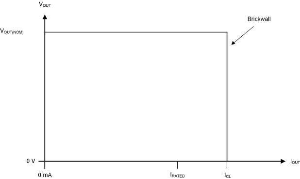
TPS7A26 tps7a26-current-limit.gifFigure 36. Current Limit