SBVS228B July 2013 – March 2015 TPS7A3501
PRODUCTION DATA.
- 1 Features
- 2 Applications
- 3 Description
- 4 Revision History
- 5 Pin Configuration and Functions
- 6 Specifications
- 7 Detailed Description
- 8 Application and Implementation
- 9 Power Supply Recommendations
- 10Layout
- 11Device and Documentation Support
- 12Mechanical, Packaging, and Orderable Information
Package Options
Mechanical Data (Package|Pins)
- DRV|6
Thermal pad, mechanical data (Package|Pins)
- DRV|6
Orderable Information
10 Layout
10.1 Layout Guidelines
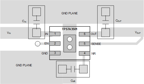
Input and output capacitors should be placed as close to the device pins as possible. TI recommends that all components be on the same side of the printed-circuit-board (PCB) as the device. Using long, thin traces or vias to connect the device to external components is highly discouraged because this practice leads to parasitic inductances, which in turn degrade noise, PSRR, and transient response. For an example layout, refer to the TPS7A3501EVM-547 Evaluation Module User Guide ( SLVU921).
10.2 Layout Example
 Figure 25. PCB Layout Example (DRV Package)
10.3 Power Dissipation
Knowing the device power dissipation and proper sizing of the thermal plane connected to the tab or pad is critical to avoiding thermal shutdown and ensuring reliable operation. Device power dissipation depends on input voltage and load conditions and can be calculated with Equation 4:
Power dissipation can be minimized and greater efficiency can be achieved by using the lowest available voltage drop option of 200 mV. However, keep in mind that higher voltage drops result in better PSRR performance.
On the WSON (DRV) package, the primary conduction path for heat is through the exposed power pad to the PCB. To ensure the device does not overheat, connect the pad to ground with an appropriate amount of copper PCB area through vias.
The maximum power dissipation determines the maximum allowable junction temperature (TJ) for the device. Power dissipation and junction temperature are most often related by the junction-to-ambient thermal resistance (θJA) of the combined PCB and device package and the temperature of the ambient air (TA), according to Equation 5:
Unfortunately, this thermal resistance (θJA) is highly dependent on the heat-spreading capability of the particular PCB design, and therefore varies according to the total copper area, copper weight, and location of the planes. The θJA recorded in the table is determined by the JEDEC standard for PCB and copper-spreading area and is to be used only as a relative measure of package thermal performance. For a well-designed thermal layout, θJA is actually the sum of the package junction-to-case (bottom) thermal resistance (θJCbot) plus the thermal resistance contribution by the PCB copper.
10.4 Estimating Junction Temperature
The JEDEC standard now recommends the use of psi (Ψ) thermal metrics to estimate the junction temperatures of the power filter on a typical PCB board application. These metrics are not strictly speaking thermal resistances, but rather offer practical and relative means of estimating junction temperatures. These psi metrics are determined to be significantly independent of copper-spreading area. The key thermal metrics (ΨJT and ΨJB) are given in the table and are used in accordance with Equation 6.

where
- PD is the power dissipated as explained in Equation 4,
- TT is the temperature at the center-top of the device package, and
- TB is the PCB surface temperature measured 1 mm from the device package and centered on the package edge.