SBVS184A December 2011 – August 2015 TPS7A4201
PRODUCTION DATA.
- 1 Features
- 2 Applications
- 3 Description
- 4 Revision History
- 5 Pin Configuration and Functions
- 6 Specifications
- 7 Detailed Description
- 8 Application and Implementation
- 9 Power Supply Recommendations
- 10Layout
- 11Device and Documentation Support
- 12Mechanical, Packaging, and Orderable Information
Package Options
Mechanical Data (Package|Pins)
- DGN|8
Thermal pad, mechanical data (Package|Pins)
- DGN|8
Orderable Information
8 Application and Implementation
NOTE
Information in the following applications sections is not part of the TI component specification, and TI does not warrant its accuracy or completeness. TI’s customers are responsible for determining suitability of components for their purposes. Customers should validate and test their design implementation to confirm system functionality.
8.1 Application Information
8.1.1 Adjustable Operation
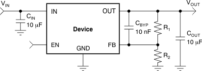
The TPS7A4201 has an output voltage range of ~1.175 V to 26 V. The nominal output voltage of the device is set by two external resistors, as shown in Figure 12.
 Figure 12. Adjustable Operation for Maximum AC Performance
R1 and R2 can be calculated for any output voltage range using the formula shown in Equation 1. To ensure stability under no-load conditions, this resistive network must provide a current greater than or equal to 10 μA.

If greater voltage accuracy is required, take into account the output voltage offset contributions because of the feedback pin current and use 0.1% tolerance resistors.
8.1.2 Transient Voltage Protection
One of the primary applications of the TPS7A4201 is to provide transient voltage protection to sensitive circuitry that may be damaged in the presence of high-voltage spikes.
This transient voltage protection can be more cost-effective and compact compared to topologies that use a transient voltage suppression (TVS) block.
8.2 Typical Application
 Figure 13. Example Circuit to Maximize Transient Performance
8.2.1 Design Requirements
For this design example, use the following parameters listed in Table 2.
Table 2. Design Parameters
| PARAMETER | VALUE |
|---|---|
| VIN | 12 V |
| VOUT | 5 V (ideal), 4.981 V (actual) |
| IOUT | 28 mA |
| Accuracy | 5 % |
| R1, R2 | 162 kΩ, 49.9 kΩ |
8.2.2 Detailed Design Procedure
The maximum value of total feedback resistance can be calculated to be 500 kΩ. Equation 1 was used to calculate R1 and R2, and standard 1% resistors were selected to keep the accuracy within the 5% allocation. 10-uF ceramic input and output capacitors were selected, along with a 10-nF bypass capacitor for optimal AC performance.
8.2.2.1 Capacitor Recommendations
Low equivalent series resistance (ESR) capacitors should be used for the input, output, and bypass capacitors. Ceramic capacitors with X7R and X5R dielectrics are preferred. These dielectrics offer more stable characteristics. Ceramic X7R capacitors offer improved over-temperature performance, while ceramic X5R capacitors are the most cost-effective and are available in higher values.
Note that high ESR capacitors may degrade PSRR.
8.2.2.2 Input and Output Capacitor Requirements
The TPS7A4101 high voltage linear regulator achieves stability with a minimum output capacitance of 4.7 µF and input capacitance of 1 µF; however, it is highly recommended to use 10-μF output and input capacitors to maximize ac performance.
8.2.2.3 Bypass Capacitor Requirements
Although a bypass capacitor (CBYP) is not needed to achieve stability, it is highly recommended to use a 10-nF bypass capacitor to maximize ac performance (including line transient, noise and PSRR).
8.2.2.4 Maximum AC Performance
In order to maximize line transient, noise, and PSRR performance, it is recommended to include 10-μF (or higher) input and output capacitors, and a 10-nF bypass capacitor; see Figure 12. The solution shown delivers minimum noise levels of 58 μVRMS and power-supply rejection levels above 36 dB from 10 Hz to 10 MHz.
8.2.2.5 Transient Response
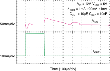
As with any regulator, increasing the size of the output capacitor reduces over/undershoot magnitude but increases duration of the transient response.
Note that the presence of the CBYP capacitor may greatly improve the TPS7A4201 line transient response, as noted in Figure 1.
8.2.3 Application Curves
