SLVSC31D December 2013 – August 2015 TPS7A4501-SP
PRODUCTION DATA.
- 1 Features
- 2 Applications
- 3 Description
- 4 Revision History
- 5 Description (continued)
- 6 Pin Configuration and Functions
- 7 Specifications
- 8 Detailed Description
- 9 Application and Implementation
- 10Power Supply Recommendations
- 11Layout
- 12Device and Documentation Support
- 13Mechanical, Packaging, and Orderable Information
Package Options
Mechanical Data (Package|Pins)
Thermal pad, mechanical data (Package|Pins)
Orderable Information
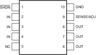
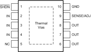
6 Pin Configuration and Functions
U Package
10-Pin CFP
Top View

HKU Package
10-Pin CFP
Top View

Pin Functions
| PIN | I/O | DESCRIPTION | |
|---|---|---|---|
| NAME | NO. | ||
| SHDN | 1 | I | Shutdown. SHDN is used to put the TPS7A4501 regulator into a low-power shutdown state. The output is off when SHDN is pulled low. SHDN can be driven by 5-V logic, 3-V logic, or open-collector logic with a pullup resistor. The pullup resistor is required to supply the pullup current of the open-collector gate, normally several microamperes, and SHDN current, typically 3 μA. If unused, the user must connect SHDN to VIN. The device is in the low-power shutdown state if SHDN is not connected. |
| IN | 2 | I | Input. Power is supplied to the device through IN. A bypass capacitor is required on this pin if the device is more than six inches away from the main input filter capacitor. In general, the output impedance of a battery rises with frequency, so it is advisable to include a bypass capacitor in battery-powered circuits. A bypass capacitor (ceramic) in the range of 1 to 10 μF is sufficient. The TPS7A4501 regulator is designed to withstand reverse voltages on IN with respect to ground and on OUT. In the case of a reverse input, which can happen if a battery is plugged in backwards, the device functions as if there is a diode in series with its input. No reverse current flows into the regulator, and no reverse voltage appears at the load. The device protects both itself and the load. |
| 3 | |||
| 4 | |||
| NC | 5 | NC | This pin is not connected to any internal circuitry. It can be left floating or tied to VIN or GND. |
| OUT | 6 | O | Output. The output supplies power to the load. To prevent oscillations, use a minimum output capacitor (ceramic) of 10 μF. Applications with large transient loads to limit peak voltage transients require larger output capacitors. |
| 7 | |||
| 8 | |||
| ADJ | 9 | I | Adjust. This is the input to the error amplifier. ADJ is internally clamped to ±7 V. It has a bias current of 3 μA that flows into the pin. ADJ voltage is 1.21 V referenced to ground, and the output voltage range is 1.21 to 20 V. |
| GND | 10 | — | Ground |
| Thermal Vias(1) | — | — | The exposed thermal vias of the HKU package should be connected to a wide ground plane for effective heat dissipation. Refer to Figure 30 and Figure 31 for the typical footprint of the HKU package. |
(1) For HKU package
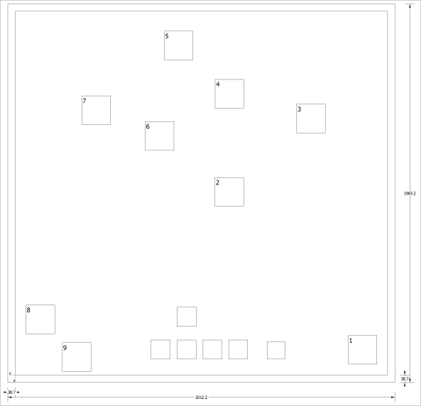
Bare Die Information
| DIE THICKNESS | BACKSIDE FINISH | BACKSIDE POTENTIAL | BOND PAD METALLIZATION COMPOSITION |
BOND PAD THICKNESS |
|---|---|---|---|---|
| 15 mils | Silicon with backgrind | Floating | TiW/AlCu2 | 1627 nm |

Bond Pad Coordinates in Microns(1)
| DESCRIPTION | PAD NUMBER | X MIN | Y MIN | X MAX | Y MAX |
|---|---|---|---|---|---|
| SHDN | 1 | 1729.25 | 55.5 | 1879.25 | 205.5 |
| IN | 2 | 1037.25 | 875 | 1187.25 | 1025 |
| IN | 3 | 1460.75 | 1255.5 | 1610.75 | 1405.5 |
| IN | 4 | 1037.75 | 1384.5 | 1187.75 | 1534.5 |
| OUT | 5 | 774.25 | 1634.75 | 924.25 | 1784.75 |
| OUT | 6 | 675.25 | 1166 | 825.25 | 1316 |
| OUT | 7 | 345.5 | 1299.25 | 495.5 | 1449.25 |
| SENSE/ADJ | 8 | 55.5 | 213 | 205.5 | 363 |
| GND | 9 | 244 | 17.5 | 394 | 167.5 |
(1) Substrate is not to be connected.