SBVS296B September   2017  – June 2018 TPS7A52-Q1

PRODUCTION DATA.  

  1. Features
  2. Applications
  3. Description
    1.     Device Images
      1.      Powering RF Components
      2.      Output Voltage Noise vs Frequency and Output Voltage
  4. Revision History
  5. Pin Configuration and Functions
    1.     Pin Functions
  6. Specifications
    1. 6.1 Absolute Maximum Ratings
    2. 6.2 ESD Ratings
    3. 6.3 Recommended Operating Conditions
    4. 6.4 Thermal Information
    5. 6.5 Electrical Characteristics
    6. 6.6 Typical Characteristics
  7. Detailed Description
    1. 7.1 Overview
    2. 7.2 Functional Block Diagram
    3. 7.3 Feature Description
      1. 7.3.1 Voltage Regulation Features
        1. 7.3.1.1 DC Regulation
        2. 7.3.1.2 AC and Transient Response
      2. 7.3.2 System Start-Up Features
        1. 7.3.2.1 Programmable Soft Start (NR/SS Pin)
        2. 7.3.2.2 Internal Sequencing
          1. 7.3.2.2.1 Enable (EN)
          2. 7.3.2.2.2 Undervoltage Lockout (UVLO) Control
          3. 7.3.2.2.3 Active Discharge
        3. 7.3.2.3 Power-Good Output (PG)
      3. 7.3.3 Internal Protection Features
        1. 7.3.3.1 Foldback Current Limit (ICL)
        2. 7.3.3.2 Thermal Protection (Tsd)
    4. 7.4 Device Functional Modes
      1. 7.4.1 Regulation
      2. 7.4.2 Disabled
      3. 7.4.3 Current Limit Operation
  8. Application and Implementation
    1. 8.1 Application Information
      1. 8.1.1  Recommended Capacitor Types
        1. 8.1.1.1 Input and Output Capacitor Requirements (CIN and COUT)
        2. 8.1.1.2 Noise-Reduction and Soft-Start Capacitor (CNR/SS)
        3. 8.1.1.3 Feed-Forward Capacitor (CFF)
      2. 8.1.2  Soft-Start and Inrush Current
      3. 8.1.3  Optimizing Noise and PSRR
      4. 8.1.4  Charge Pump Noise
      5. 8.1.5  Current Sharing
      6. 8.1.6  Adjustable Operation
      7. 8.1.7  Power-Good Operation
      8. 8.1.8  Undervoltage Lockout (UVLO) Operation
      9. 8.1.9  Dropout Voltage (VDO)
      10. 8.1.10 Load Transient Response
      11. 8.1.11 Reverse Current Protection Considerations
      12. 8.1.12 Power Dissipation (PD)
      13. 8.1.13 Estimating Junction Temperature
    2. 8.2 Typical Application
      1. 8.2.1 Design Requirements
      2. 8.2.2 Detailed Design Procedure
      3. 8.2.3 Application Curves
  9. Power Supply Recommendations
  10. 10Layout
    1. 10.1 Layout Guidelines
      1. 10.1.1 Board Layout
      2. 10.1.2 RTK Package—High CTE Mold Compound
    2. 10.2 Layout Example
  11. 11Device and Documentation Support
    1. 11.1 Device Support
      1. 11.1.1 Development Support
        1. 11.1.1.1 Evaluation Modules
        2. 11.1.1.2 Reference Designs
        3. 11.1.1.3 Spice Models
      2. 11.1.2 Device Nomenclature
    2. 11.2 Documentation Support
      1. 11.2.1 Related Documentation
    3. 11.3 Receiving Notification of Documentation Updates
    4. 11.4 Support Resources
    5. 11.5 Trademarks
    6. 11.6 Electrostatic Discharge Caution
    7. 11.7 Glossary
  12. 12Mechanical, Packaging, and Orderable Information

Package Options

Mechanical Data (Package|Pins)
Thermal pad, mechanical data (Package|Pins)
Orderable Information

Mechanical, Packaging, and Orderable Information

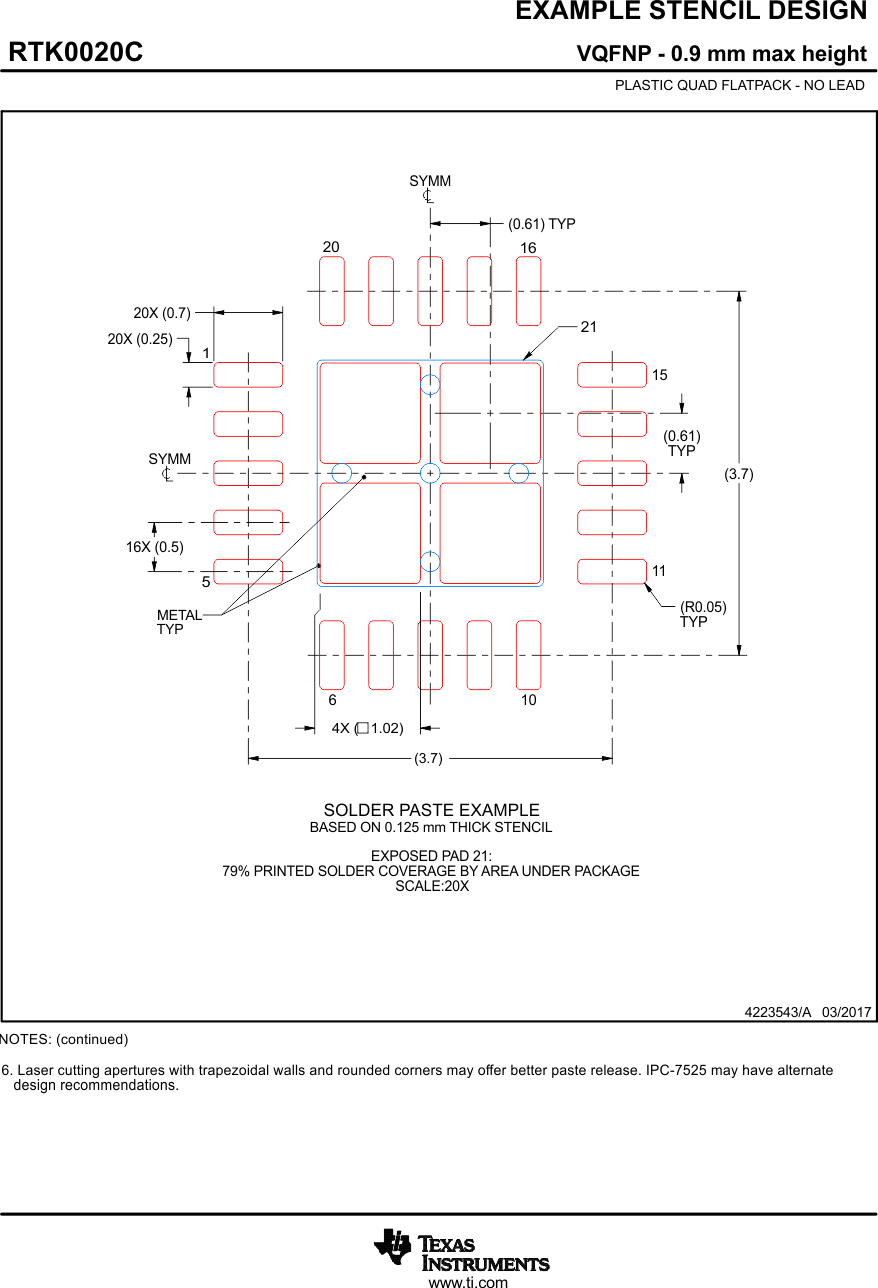
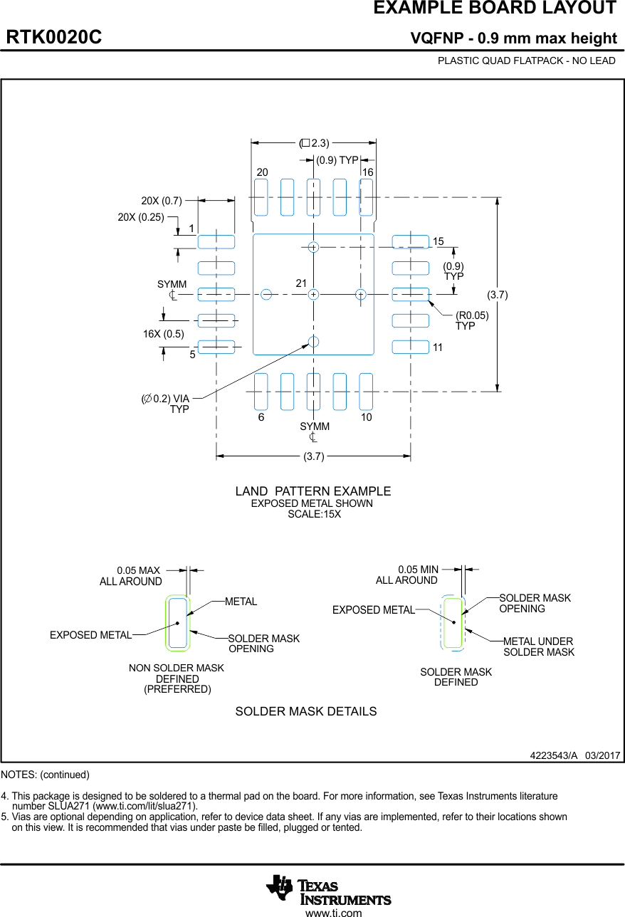
The following pages include mechanical, packaging, and orderable information. This information is the most current data available for the designated devices. This data is subject to change without notice and revision of this document. For browser-based versions of this data sheet, refer to the left-hand navigation.
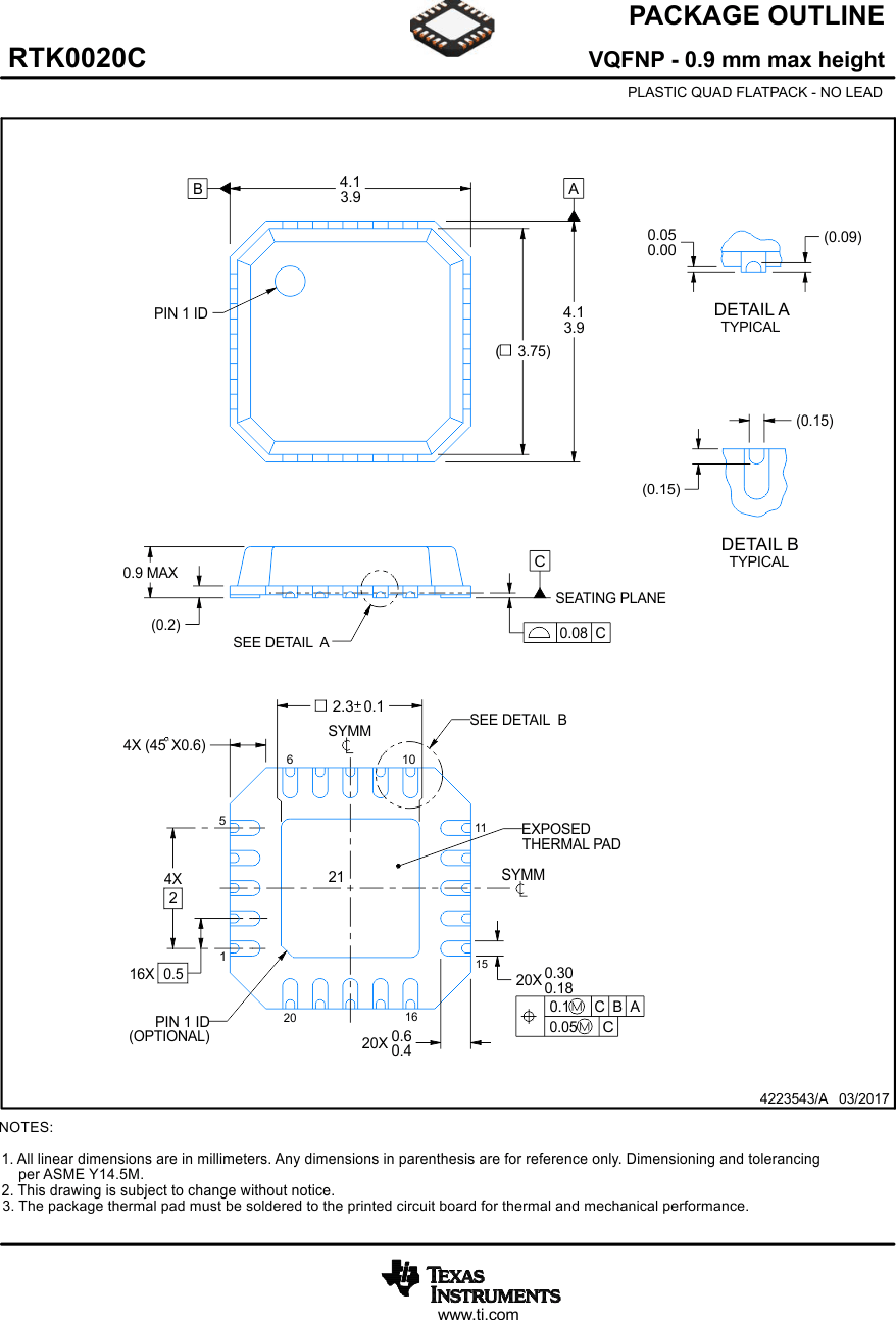
TPS7A52-Q1 RTK0020C_4223543_Page_01.gif
TPS7A52-Q1 RTK0020C_4223543_Page_02.gif
TPS7A52-Q1 RTK0020C_4223543_Page_03.gif