SLVSA62J March   2010  – March 2020 TPS7A60-Q1 , TPS7A61-Q1

PRODUCTION DATA.  

  1. Features
  2. Applications
  3. Description
    1.     Device Images
      1.      Programmable Reset Delay Option
      2.      Enable Option
  4. Revision History
  5. Device Comparison Table
  6. Pin Configuration and Functions
    1.     Pin Functions
  7. Specifications
    1. 7.1 Absolute Maximum Ratings
    2. 7.2 ESD Ratings
    3. 7.3 Recommended Operating Conditions
    4. 7.4 Thermal Information
    5. 7.5 Electrical Characteristics
    6. 7.6 Switching Characteristics
    7. 7.7 Typical Characteristics
  8. Detailed Description
    1. 8.1 Overview
    2. 8.2 Functional Block Diagrams
    3. 8.3 Feature Description
      1. 8.3.1 Reset Delay and Reset Output
      2. 8.3.2 Charge Pump Operation
      3. 8.3.3 Undervoltage Shutdown
      4. 8.3.4 Low-Voltage Tracking
      5. 8.3.5 Integrated Fault Protection
      6. 8.3.6 Thermal Shutdown
    4. 8.4 Device Functional Modes
      1. 8.4.1 Low-Power Mode
      2. 8.4.2 Sleep Mode (TPS7A61-Q1 Only)
      3. 8.4.3 Regulation Mode
  9. Application and Implementation
    1. 9.1 Application Information
    2. 9.2 Typical Applications
      1. 9.2.1 TPS7A60-Q1 Typical Application
        1. 9.2.1.1 Design Requirements
        2. 9.2.1.2 Detailed Design Procedure
          1. 9.2.1.2.1 Input Capacitor
          2. 9.2.1.2.2 Output Capacitor
        3. 9.2.1.3 Application Curve
      2. 9.2.2 TPS7A61-Q1 Typical Application
        1. 9.2.2.1 Design Requirements
        2. 9.2.2.2 Detailed Design Procedure
        3. 9.2.2.3 Application Curve
  10. 10Power Supply Recommendations
  11. 11Layout
    1. 11.1 Layout Guidelines
      1. 11.1.1 Power Dissipation and Thermal Considerations
    2. 11.2 Layout Examples
  12. 12Device and Documentation Support
    1. 12.1 Related Links
    2. 12.2 Receiving Notification of Documentation Updates
    3. 12.3 Community Resources
    4. 12.4 Trademarks
    5. 12.5 Electrostatic Discharge Caution
    6. 12.6 Glossary
  13. 13Mechanical, Packaging, and Orderable Information

Package Options

Mechanical Data (Package|Pins)
Thermal pad, mechanical data (Package|Pins)
Orderable Information

Charge Pump Operation

These devices have an internal charge pump which turns on or off depending on the input voltage and the output current. The charge-pump switching circuitry does not cause conducted emissions to exceed required thresholds on the input-voltage line. For a given output current, the charge pump stays on at lower input voltages and turns off at higher input voltages. The charge-pump switching thresholds are hysteretic. Figure 19 and Figure 20 show typical switching thresholds for the charge pump at light (IOUT < approximately 2 mA) and heavy (IOUT > approximately 2 mA) loads, respectively.
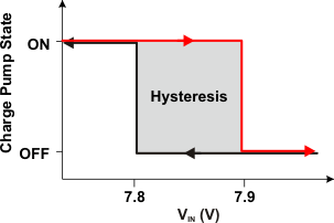
TPS7A60-Q1 TPS7A61-Q1 charge_pump_light_load_lvsa62.gifFigure 19. Charge Pump Operation at Light Loads
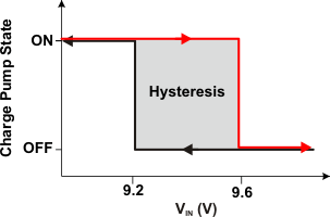
TPS7A60-Q1 TPS7A61-Q1 charge_pump_heavy_load_lvsa62.gifFigure 20. Charge Pump Operation at Heavy Loads