SBVS190F March   2012  – October 2023 TPS7A7300

PRODUCTION DATA  

  1.   1
  2. Features
  3. Applications
  4. Description
  5. Pin Configurations
  6. Specifications
    1. 5.1 Absolute Maximum Ratings
    2. 5.2 ESD Ratings
    3. 5.3 Recommended Operating Conditions
    4. 5.4 Thermal Information
    5. 5.5 Electrical Characteristics
    6. 5.6 Typical Characteristics
  7. Detailed Description
    1. 6.1 Overview
    2. 6.2 Functional Block Diagram
    3. 6.3 Feature Description
      1. 6.3.1 User-Configurable Output Voltage
      2. 6.3.2 Traditional Adjustable Configuration
      3. 6.3.3 Undervoltage Lockout (UVLO)
      4. 6.3.4 Soft-Start
      5. 6.3.5 Current Limit
      6. 6.3.6 Enable
      7. 6.3.7 Power-Good
    4. 6.4 Device Functional Modes
      1. 6.4.1 Normal Operation
      2. 6.4.2 Dropout Operation
      3. 6.4.3 Disabled
  8. Application and Implementation
    1. 7.1 Application Information
    2. 7.2 Typical Application
      1. 7.2.1 Design Requirements
      2. 7.2.2 Detailed Design Procedure
        1. 7.2.2.1 ANY-OUT Programmable Output Voltage
        2. 7.2.2.2 Traditional Adjustable Output Voltage
        3. 7.2.2.3 Input Capacitor Requirements
        4. 7.2.2.4 Output Capacitor Requirements
      3. 7.2.3 Application Curves
    3. 7.3 Power Supply Recommendations
    4. 7.4 Layout
      1. 7.4.1 Layout Guidelines
        1. 7.4.1.1 Thermal Considerations
        2. 7.4.1.2 Power Dissipation
        3. 7.4.1.3 Estimating Junction Temperature
      2. 7.4.2 Layout Example
  9. Device And Documentation Support
    1. 8.1 Documentation Support
      1. 8.1.1 Related Documentation
    2. 8.2 Receiving Notification of Documentation Updates
    3. 8.3 Support Resources
    4. 8.4 Trademarks
    5. 8.5 Electrostatic Discharge Caution
    6. 8.6 Glossary
  10. Revision History
  11. 10Mechanical, Packaging, And Orderable Information

Package Options

Refer to the PDF data sheet for device specific package drawings

Mechanical Data (Package|Pins)
  • RGW|20
Thermal pad, mechanical data (Package|Pins)
Orderable Information

Description

The TPS7A7300 low-dropout (LDO) voltage regulator is designed for applications requiring very-low dropout capability (240 mV at 3 A) with an input voltage from 1.5 V to 6.5 V. The TPS7A7300 offers an innovative, user-configurable, output-voltage setting from 0.9 V to 3.5 V, thus eliminating external resistors and any associated errors.

The TPS7A7300 has very fast load-transient response, is stable with ceramic output capacitors, and supports a better than 2% accuracy over line, load, and temperature. A soft-start pin allows for an application to reduce inrush into the load. Additionally, an open-drain, power-good signal allows for sequencing power rails.

The TPS7A7300 is available in a 5-mm × 5-mm, 20-pin VQFN package.
Package Information
PART NUMBER PACKAGE(1) PACKAGE SIZE(2)
TPS7A7300 RGW (VQFN, 20) 5 mm × 5 mm
For all available packages, see the orderable addendum at the end of the data sheet.
The package size (length × width) is a nominal value and includes pins, where applicable.


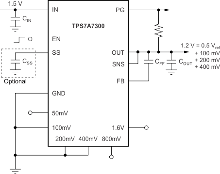
GUID-4FEFEE68-3458-4243-9ED1-C13793C514EB-low.gifTypical Application
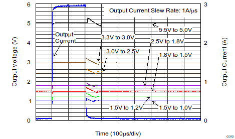
GUID-2725943A-FEFE-42E1-A4FD-9C18C06818D4-low.pngLoad Transient Response With Seven Different Outputs