SBVS190F March   2012  – October 2023 TPS7A7300

PRODUCTION DATA  

  1.   1
  2. Features
  3. Applications
  4. Description
  5. Pin Configurations
  6. Specifications
    1. 5.1 Absolute Maximum Ratings
    2. 5.2 ESD Ratings
    3. 5.3 Recommended Operating Conditions
    4. 5.4 Thermal Information
    5. 5.5 Electrical Characteristics
    6. 5.6 Typical Characteristics
  7. Detailed Description
    1. 6.1 Overview
    2. 6.2 Functional Block Diagram
    3. 6.3 Feature Description
      1. 6.3.1 User-Configurable Output Voltage
      2. 6.3.2 Traditional Adjustable Configuration
      3. 6.3.3 Undervoltage Lockout (UVLO)
      4. 6.3.4 Soft-Start
      5. 6.3.5 Current Limit
      6. 6.3.6 Enable
      7. 6.3.7 Power-Good
    4. 6.4 Device Functional Modes
      1. 6.4.1 Normal Operation
      2. 6.4.2 Dropout Operation
      3. 6.4.3 Disabled
  8. Application and Implementation
    1. 7.1 Application Information
    2. 7.2 Typical Application
      1. 7.2.1 Design Requirements
      2. 7.2.2 Detailed Design Procedure
        1. 7.2.2.1 ANY-OUT Programmable Output Voltage
        2. 7.2.2.2 Traditional Adjustable Output Voltage
        3. 7.2.2.3 Input Capacitor Requirements
        4. 7.2.2.4 Output Capacitor Requirements
      3. 7.2.3 Application Curves
    3. 7.3 Power Supply Recommendations
    4. 7.4 Layout
      1. 7.4.1 Layout Guidelines
        1. 7.4.1.1 Thermal Considerations
        2. 7.4.1.2 Power Dissipation
        3. 7.4.1.3 Estimating Junction Temperature
      2. 7.4.2 Layout Example
  9. Device And Documentation Support
    1. 8.1 Documentation Support
      1. 8.1.1 Related Documentation
    2. 8.2 Receiving Notification of Documentation Updates
    3. 8.3 Support Resources
    4. 8.4 Trademarks
    5. 8.5 Electrostatic Discharge Caution
    6. 8.6 Glossary
  10. Revision History
  11. 10Mechanical, Packaging, And Orderable Information

Package Options

Refer to the PDF data sheet for device specific package drawings

Mechanical Data (Package|Pins)
  • RGW|20
Thermal pad, mechanical data (Package|Pins)
Orderable Information

Application Curves

GUID-51506462-8FC0-478F-BDFC-65749EC3D20F-low.png
 
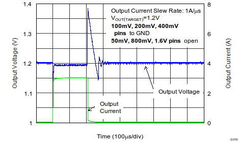
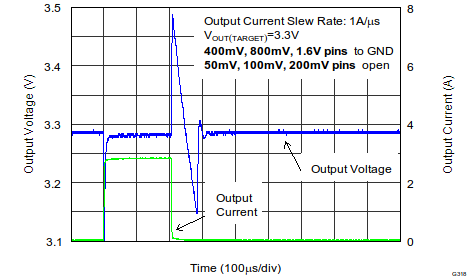
Figure 7-2 Load Transient Response (VOUT = 1.2 V)
GUID-AA891DBC-6F2C-4204-8010-94CCC5E542B9-low.png
 
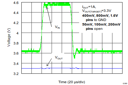
Figure 7-4 Line Transient Response
GUID-F6C86C21-81CC-45DF-9288-947B11C5D161-low.png
 
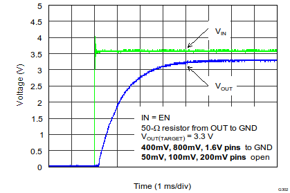
Figure 7-6 Turnon Response (IN = EN)
GUID-BF4042E3-9BE5-4A45-9059-79FE69B2FC76-low.png
 
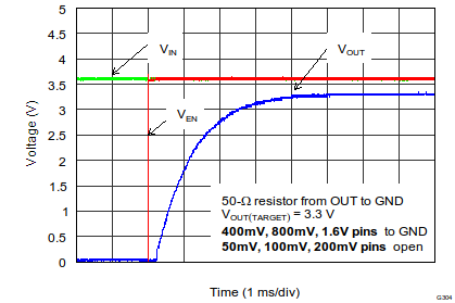
Figure 7-8 EN Pulse On Response (Over Stable VIN)
GUID-10C4B0A2-0DB8-4A21-A0CA-6C1AEB5A16D4-low.png
 
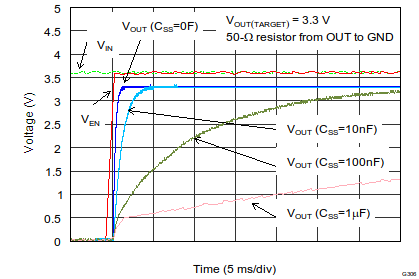
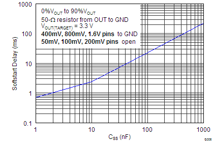
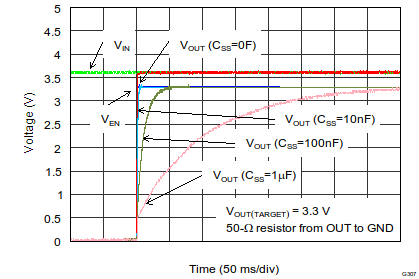
Figure 7-10 Soft-Start Delay vs CSS (Enlarged View)
GUID-67A6B0A6-92FA-4994-9F01-31A896E4695E-low.png
 
Figure 7-12 Soft-Start Delay vs CSS
GUID-52647C8B-6DFA-489A-B5C3-397EB2FD2BA2-low.png
 
Figure 7-3 Load Transient Response (VOUT = 3.3 V)
GUID-E71753A7-0B82-406E-A553-A293ED48E68F-low.png
 
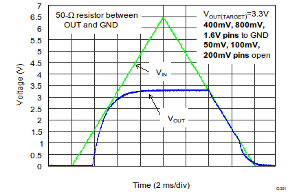
Figure 7-5 Power Up and Power Down (IN = EN)
GUID-DDABE911-A8BC-454D-8650-900E9ED10390-low.png
 
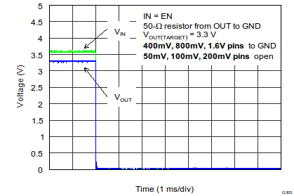
Figure 7-7 Turnoff Response (IN = EN)
GUID-EBEFFBEE-5979-44BB-B901-537C1316803B-low.png
 
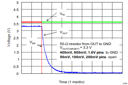
Figure 7-9 EN Pulse Off Response (Over Stable VIN)
GUID-1CC68C6C-F84C-481B-AAC7-9AB5C7111E52-low.png
 
Figure 7-11 Soft-Start Delay vs CSS (Reduced View)