SLVSCK0A April 2014 – June 2014 TPS7A8101-Q1
PRODUCTION DATA.
- 1 Features
- 2 Applications
- 3 Description
- 4 Typical Application Circuit
- 5 Revision History
- 6 Pin Configuration and Functions
- 7 Specifications
- 8 Detailed Description
- 9 Application and Implementation
- 10Power Supply Recommendations
- 11Layout
- 12Device and Documentation Support
- 13Mechanical, Packaging, and Orderable Information
Package Options
Mechanical Data (Package|Pins)
- DRB|8
Thermal pad, mechanical data (Package|Pins)
- DRB|8
Orderable Information
9 Application and Implementation
9.1 Application Information
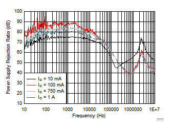
The TPS7A8101-Q1 device belongs to a family of new-generation LDO regulators that use innovative circuitry to achieve wide bandwidth and high loop gain, resulting in extremely high PSRR (over a 1-MHz range) even with very low headroom (VI – VO). A noise-reduction capacitor (C(NR)) at the NR pin and a bypass capacitor (C(BYPASS)) decrease noise generated by the bandgap reference in order to improve PSRR, while a quick-start circuit fast-charges the noise-reduction capacitor. This family of regulators offers sub-bandgap output voltages, current-limit, and thermal protection, and is fully specified from –40°C to 125°C.
9.2 Typical Application
Figure 31 shows the connections for the device.
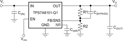 Figure 31. Typical Application Circuit
The voltage on the FB pin sets the output voltage and is determined by the values of the resistors R1 and R2. Use Equation 2 to calculate the values of R1 and R2 any voltage.
Table 1 lists sample resistor values for common output voltages. In Table 1, E96 series resistors are used, and all values meet 1% of the target VO, assuming resistors with zero error. For the actual design, pay attention to any resistor error-factors. Using lower values for R1 and R2 reduces the noise injected into the FB pin.
9.2.1 Design Requirements
9.2.1.1 Dropout Voltage
The TPS7A8101-Q1 device uses a PMOS pass transistor to achieve low dropout. When (VI – VOnom) is less than the dropout voltage (VDO), the PMOS pass device is in the linear region of operation and the input-to-output resistance is the rDS(on) of the PMOS pass element. VDO is proportional to the output current because the PMOS device in dropout functions in the same way as a resistor.
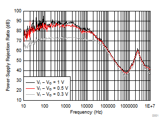
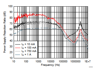
As with any linear regulator, PSRR and transient responses are degraded as (VI – VO) approaches dropout. Figure 19 and Figure 20 in the Typical Characteristics section shown this effect.
9.2.1.2 Minimum Load
The TPS7A8101-Q1 device is stable and functions well with no output load. Traditional PMOS-LDO regulators suffer from lower loop gain at very light output loads. The TPS7A8101-Q1 device employs an innovative low-current mode circuit to increase loop gain under very light or no-load conditions, resulting in improved output voltage regulation performance down to zero output current.
9.2.1.3 Input And Output Capacitor Requirements
Although an input capacitor is not required for stability, connecting a 0.1-µF to 1-µF low-equivalent series-resistance (ESR) capacitor from the input supply near the regulator to ground is good analog-design practice. This capacitor counteracts reactive input sources and improves transient response and ripple rejection. A higher-value capacitor may be necessary if large, fast load transients are anticipated or if the device is located several inches from the power source. If source impedance is not sufficiently low, a 0.1-μF input capacitor may be necessary to ensure stability.
The TPS7A8101-Q1 device is designed to be stable with standard ceramic capacitors of capacitance values 4.7 μF or larger. This device was evaluated using a 10-μF ceramic capacitor of 10-V rating, 10% tolerance, X5R type, and 0805 size (2 mm × 1,25 mm).
X5R-type and X7R-type capacitors are highly recommended because they have minimal variation in capacitance and ESR over temperature. The maximum ESR should be less than 1 Ω.
Table 1. Recommended Feedback Resistor Values for Common Output Voltages
| VO | R1 | R2 |
|---|---|---|
| 0.8 V | 0 Ω (Short) | 10 kΩ |
| 1 V | 2.49 kΩ | 10 kΩ |
| 1.2 V | 4.99 kΩ | 10 kΩ |
| 1.5 V | 8.87 kΩ | 10 kΩ |
| 1.8 V | 12.5 kΩ | 10 kΩ |
| 2.5 V | 21 kΩ | 10 kΩ |
| 3.3 V | 30.9 kΩ | 10 kΩ |
| 5 V | 52.3 kΩ | 10 kΩ |
Table 2. Recommended Capacitor Values
| NAME | DESCRIPTION | VALUE |
|---|---|---|
| C(NR) | Noise-reduction capacitor between the NR and GND pins | 470 nF |
| C(BYPASS) | Noise-reduction capacitor across R1 | 470 nF |
| C(OUTPUT) | Output capacitor | 10 µF |
| C(IN) | Input capacitor | 10 µF |
9.2.1.4 Transient Response
As with any regulator, increasing the size of the output capacitor reduces overshoot and undershoot magnitude but increases the duration of the transient response. Using a larger noise-reduction capacitor (C(NR)), bypass capacitor (C(BYPASS)), or both types of capacitors can improve line-transient performance.
9.2.2 Detailed Design Procedure
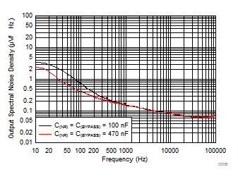
9.2.2.1 Output Noise
In most LDOs, the bandgap is the dominant noise source. If a noise reduction capacitor (C(NR)) is used with the TPS7A8101-Q1 device, the bandgap does not contribute significantly to noise. Instead, noise is dominated by the output resistor-divider and the error-amplifier input. If a bypass capacitor (C(BYPASS)) across the high-side feedback resistor (R1) is used with the TPS7A8101-Q1 device, noise from these other sources can also be significantly reduced.
To maximize noise performance in a given application, use a 0.47-μF noise-reduction capacitor plus a 0.47-μF bypass capacitor.
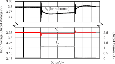
9.2.3 Application Curves
| C(NR) = C(BYPASS) = 470 nF | C(OUT) = 10 µF | C(IN) = 0 F |
| VI – VO = 0.5 V | C(IN) = 0 F | C(OUT) = 10 µF |
| C(NR) = C(BYPASS) = 470 nF | ||
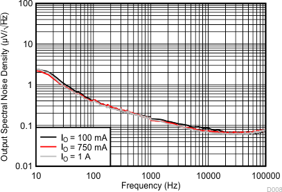
| 23.54 µVRMS (IO = 100 mA) | C(IN) = 10 µF | VI – VO = 0.5 V |
| 23.71 µVRMS (IO = 750 mA) | C(NR) = 470 nF | C(OUT) = 10 µF |
| 22.78 µVRMS (IO = 1 A) | C(BYPASS) = 470 nF | |
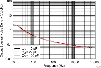
| 23.54 µVRMS (CO = 10 µF) | C(IN) = 10 µF | VI – VO = 0.5 V |
| 23.91 µVRMS (CO = 22 µF) | C(NR) = 470 nF | C(OUT) = 10 µF |
| 22.78 µVRMS (CO = 100 µF) | C(BYPASS) = 470 nF | |
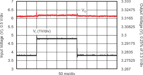
| VI = 3.8 V → 4.8 V → 3.8 V | ||
| IO = 500 mA | ||
| RL = 33 Ω | C(NR) = 470 nF | C(BYPASS) = 470 nF |
| C(OUT) = 10 µF | C(IN) = 10 µF | |
| VI – VO = 1 V | C(IN) = 0 F | C(OUT) = 10 µF |
| C(NR) = C(BYPASS) = 470 nF | ||
| VI – VO = 0.5 V | C(OUT) = 10 µF | C(IN) = 10 µF | |
| 24.09 µVRMS (C(NR) = C(BYPASS) = 100 nF) | |||
| 23.54 µVRMS (C(NR) = C(BYPASS) = 470 nF) | |||
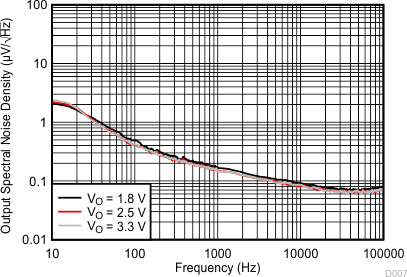
| 25.89 µVRMS (VO = 1.8 V) | C(IN) = 10 µF | VI – VO = 0.5 V |
| 23.54 µVRMS (VO = 2.5 V) | C(NR) = 470 nF | C(OUT) = 10 µF |
| 23.54 µVRMS (VO = 3.3 V) | C(BYPASS) = 470 nF | |
| Using the same value of C(NR) and C(BYPASS) in the X-Axis | ||
| IO = 100 mA → 1 A → 100 mA | ||
| RL = 33 Ω | C(NR) = 470 nF | C(BYPASS) = 470 nF |
| C(OUT) = 10 µF | C(IN) = 10 µF | |
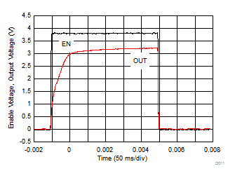
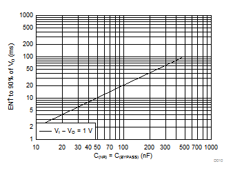
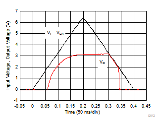
| (1) The internal reference requires approximately 80 ms of rampup time (see Startup) from the enable event; therefore, VO fully reaches the target output voltage of 3.3 V in 80 ms from startup. | ||